Non-volatile memory structure

a memory structure and non-volatile technology, applied in the field of non-volatile memory arrays, can solve the problems of complicated whole test process, additional processes,

Inactive Publication Date: 2009-03-31
SILICON MOTION INC (TW)
View PDF11 Cites 0 Cited by
  • Summary
  • Abstract
  • Description
  • Claims
  • Application Information

AI Technical Summary

Benefits of technology

[0011]It is therefore an aspect of the present invention to provide a non-volatile memory array structure, which can disable the connection between failed bit lines and the sense amplifier during the first wafer sort stage to omit the laser repair and the second wafer sort process.
[0015]As mentioned above, the connections between the failed bit lines and the sense amplifier is disabled during the first wafer stage, so the laser repair and second wafer sorting process are no longer necessary such that the test can be simpler.

Problems solved by technology

However, additional processes will be needed if the laser trimming method is used.
These additional steps make the whole test process more complicated.

Method used


Image

  • Non-volatile memory structure
  • Non-volatile memory structure
  • Non-volatile memory structure

Examples


Embodiment Construction

[0021]Reference is made in detail to the present embodiments of the invention, examples of which are illustrated in the accompanying drawings. Wherever possible, the same reference numbers are used in the drawings and the description to refer to the same or like parts.

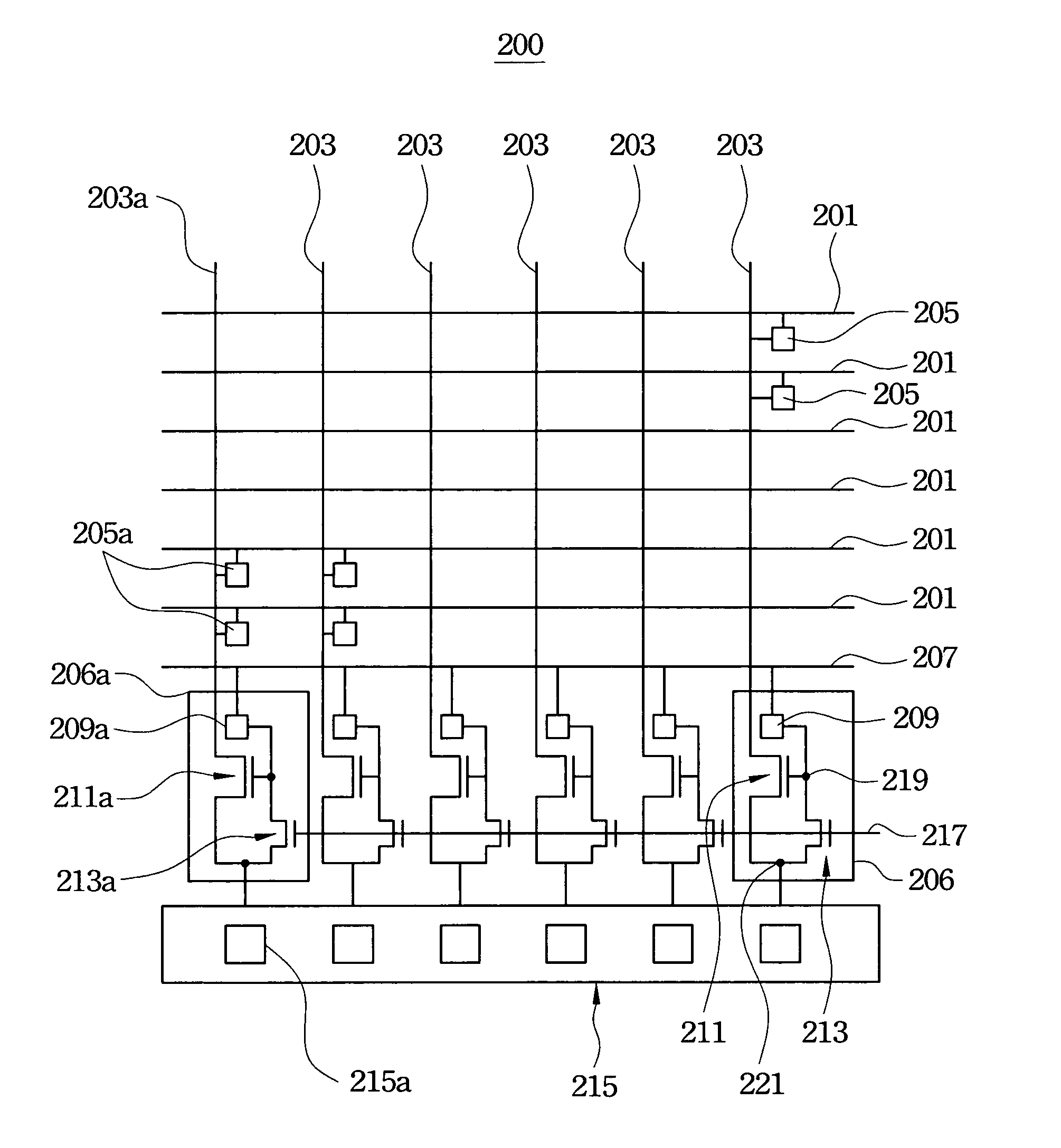
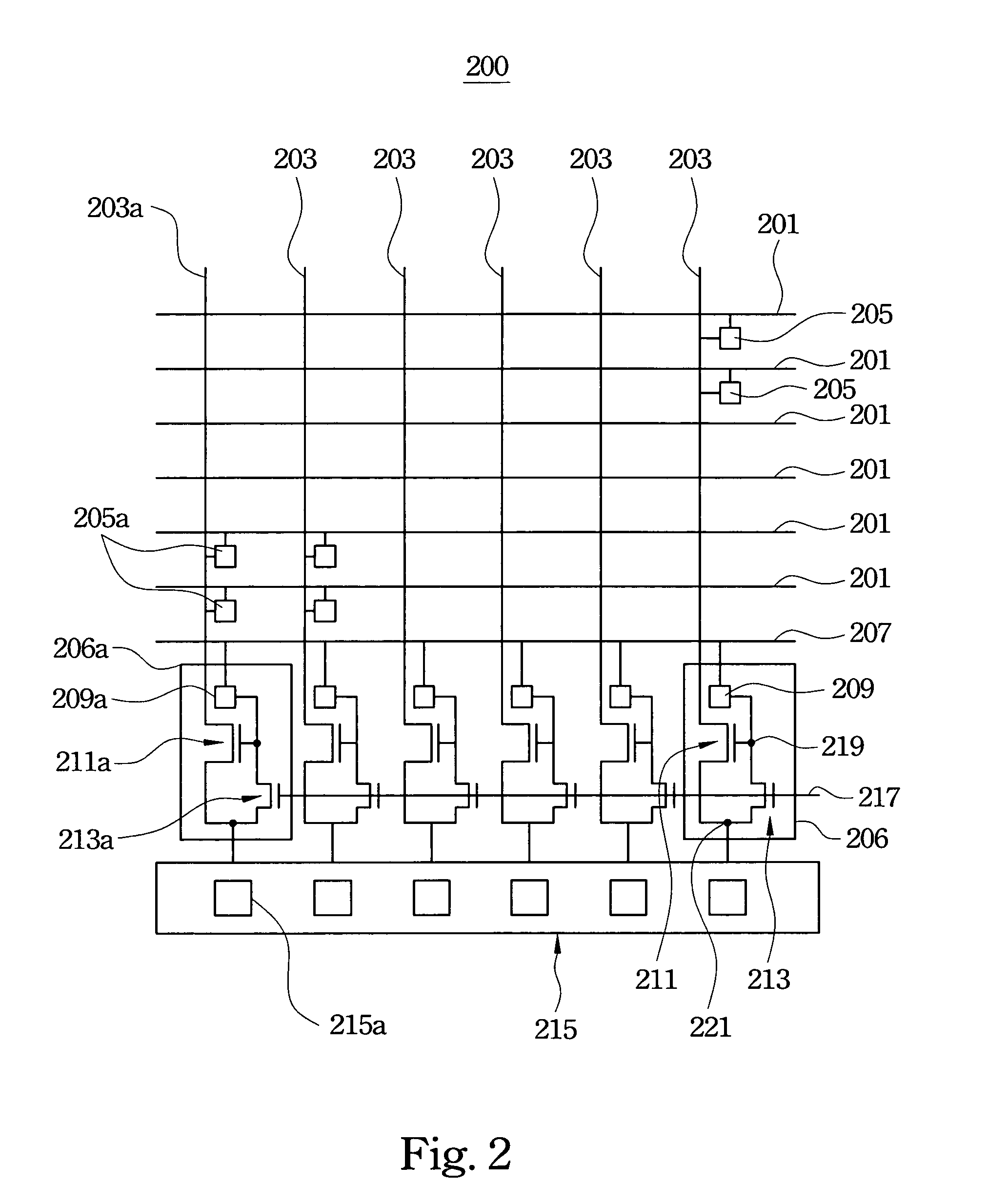
[0022]FIG. 2 is a schematic view of a non-volatile memory structure of one embodiment of the present invention. The non-volatile memory structure 200 includes N bit lines 203, M first word lines 201, M×N first memory cells 205, a second word line 207, n repair circuits 206 and a sense amplifier 215. The N bit lines 203 and M first word lines 201 are interlaced to control the M×N first memory cells 205. The second word line 207 is placed across the n bit lines 203. Among above, the M and N are natural number.

[0023]Each repair circuit 206 is electrically connected between one of the bit lines 203 and the sense amplifier 215, each of which includes a second memory cell 209, a first transistor 211 and a second transistor 2...


PUM


Abstract

A non-volatile memory array structure includes N bit lines, M first word lines, M×N first memory cells, a second word line, n repair circuits and a sense amplifier. The N bit lines and M first word lines are interlaced to control the M×N first memory cell. The second word line is placed across the n bit lines. Each of the repair circuits is electrically connected between the corresponding bit line and the sense amplifier. M and N are natural number.

Description

RELATED APPLICATIONS[0001]The present application is based on, and claims priority from, Taiwan Application Serial Number 95123218, filed Jun. 27, 2006, the disclosure of which is hereby incorporated by reference herein in its entirety.BACKGROUND[0002]1. Field of Invention[0003]The present invention relates to nonvolatile memory array. More particularly, the present invention relates to nonvolatile memory array without a fuse.[0004]2. Description of Related Art[0005]Non-volatile memory devices, such as flash, include a floating gate to store electric charge and a charge input / output control unit. Flash can be used for Basic Input Output System (BIOS) of a computer, high-density non-volatile memory array can be applied to mass storage devices in a portable Terminal Server, digital camera and memory card of a computer. Non-volatile memory has a lot of advantages, such as quick operation time, low power consumption and durability. A chip probing process is taken to test if the non-vola...

Claims


Application Information

Patent Timeline
Patent Type & Authority Patents(United States)
IPC IPC(8): G11C11/00
CPCG11C29/78G11C29/832G11C29/006H10B63/80
Inventor CHEN, TE-WEI
Owner SILICON MOTION INC (TW)
Why Eureka
Try Eureka