Independently-double-gated field effect transistor

a field effect transistor and independent technology, applied in the direction of logic circuits, pulse techniques, semiconductor devices, etc., can solve the problems of increasing secondary effects, increasing problems, and reducing the influence of gate voltage on the channel, so as to achieve dynamically reduce static power and low static power

a field effect transistor and independent technology, applied in the direction of logic circuits, pulse techniques, semiconductor devices, etc., can solve the problems of increasing secondary effects, increasing problems, and reducing the influence of gate voltage on the channel, so as to achieve dynamically reduce static power and low static power

US7518189B1Active Publication Date: 2009-04-14AMERICAN SEMICON

Image

  • Independently-double-gated field effect transistor
  • Independently-double-gated field effect transistor
  • Independently-double-gated field effect transistor

Examples


Embodiment Construction

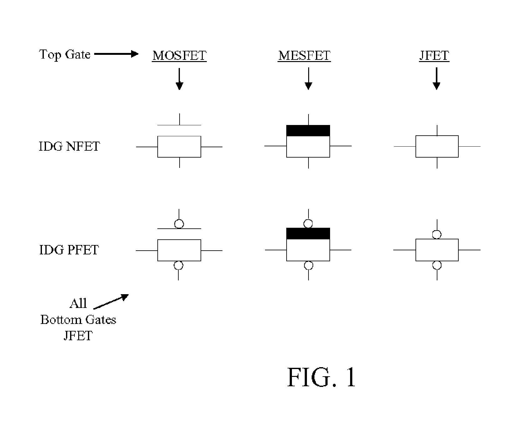
[0062]A variety of independently double-gated (IDG) field effect transistors (FETs) are depicted in FIG. 1. There are three possible types of IDG FETs, having either MOSFET, MESFET, or JFET top gates.

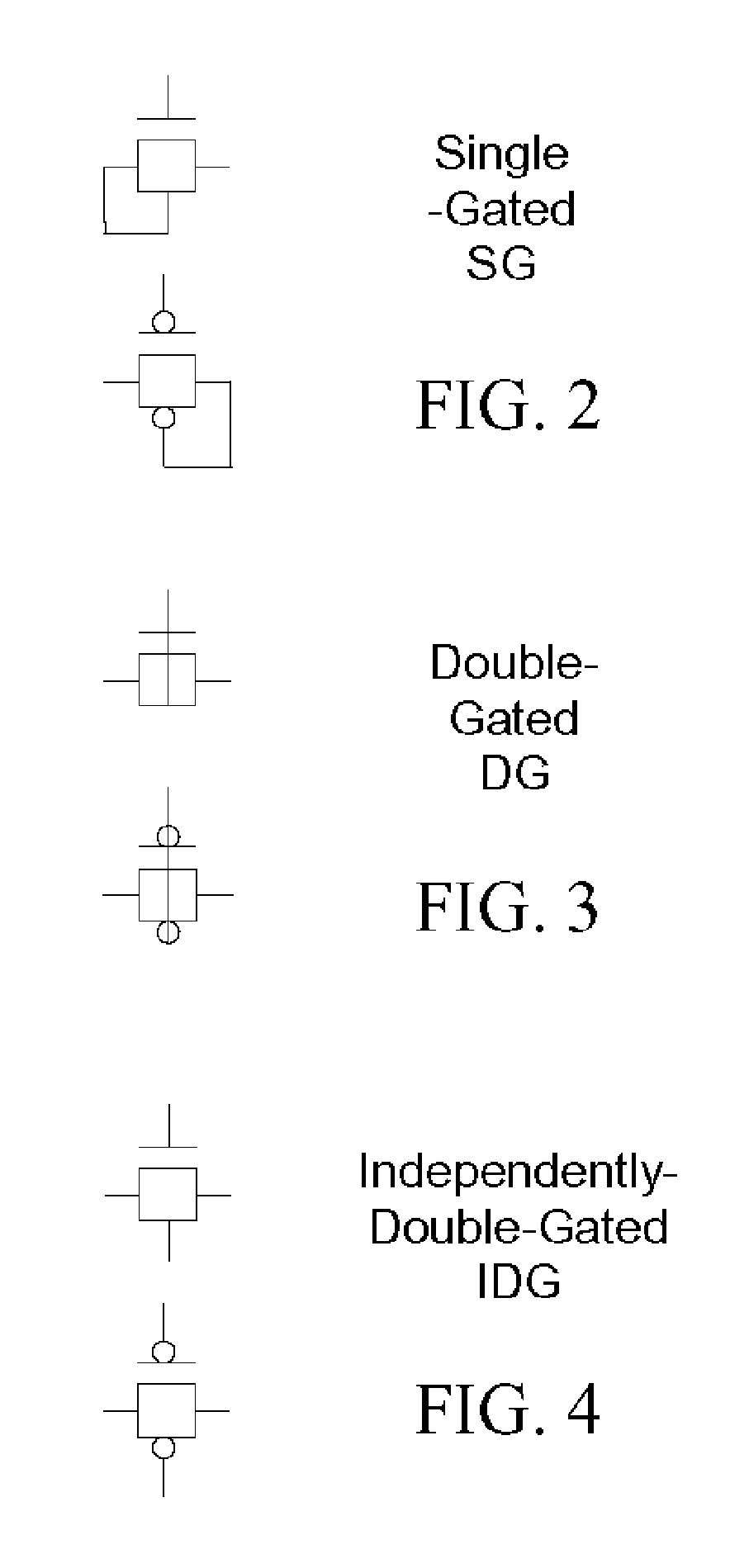
[0063]FIGS. 2-4 show schematic representations of various IDGFET embodiments. FIG. 2 shows both n-channel and p-channel single gated (SG) versions of devices having an MOS topgate with a JFET bottomgate. In this SG configuration the bottomgate is connected to the source, or it may be left to float. The double-gated (DG) transistors of FIG. 3 have their top and bottom gates connected together, as is the case with conventional double-gated transistors. The independently double-gated (IDG) transistors of FIG. 4 are true four-terminal devices, providing independent bias to the topgate and the bottomgate. As is well known in the art, each device represented in FIGS. 2-4 has specific uses that are suitable for different applications.

[0064]With the freedom to design using a true four-terminal ...


PUM


Abstract

This independent double-gated transistor architecture creates a MOSFET, JFET or MESFET in parallel with a JFET. Its two gates may be configured to provide a four-terminal device for independent gate control, a floating gate device, and a double-gate device. First and second insulating spacers are disposed on opposing sides of the top gate with the first spacer between the source and the top gate and the second spacer between the drain and the top gate. Source and drain extensions extend proximate to the spacers and couple to the channel. The spacers shield the channel from the field effect of the source and drain and further resist compression of the channel by the source and drain. Truly independent control of the two gates makes possible many 2-, 3- and 4-terminal device configurations that may be dynamically reconfigured to trade off speed against power. The resulting transistors exhibit inherent radiation tolerance.

Description

CROSS-REFERENCES TO RELATED APPLICATIONS[0001]This application is a Continuation-In-Part of U.S. patent application Ser. No. 10 / 613,169 filed Jul. 3, 2003, entitled “Multi-Configurable Independently Double-Gated MOSFET,” which is incorporated here by reference.FIELD OF THE INVENTION[0002]The present invention relates generally to the structure and application of field effect transistors in which current flow through a channel is controlled by more than one gate electrode. More particularly, the present invention pertains to field effect transistors in which a single channel is controlled independently by two gates, at least one of which is a junction gate.BACKGROUND OF THE INVENTION[0003]Circuit design engineers within the dynamic electronics industry are constantly looking for components that are smaller and more efficient. Ever-increasing device densities have been driven by demand for ever-increasingly capable products that require more and more memory to support ever more comple...

Claims


Application Information

Patent Timeline
14 Apr 2009
Publication
US7518189B1
IPC
H01L29/94
CPC
H01L21/2256; H01L21/823437; H01L21/84; H01L27/088; H01L27/098; H01L27/1203; H01L29/4908; H01L29/66484
Inventors
HACKLER, SR., DOUGLAS R.; PARKE, STEPHEN A.