Semiconductor memory device, and data transmitting/receiving system
a memory device and memory technology, applied in the field of semiconductor memory devices, can solve the problems of increasing the total number of terminals, and achieve the effect of preventing the information processing device from running out of control
- Summary
- Abstract
- Description
- Claims
- Application Information
AI Technical Summary
Benefits of technology
Problems solved by technology
Method used
Image
Examples
embodiment 1
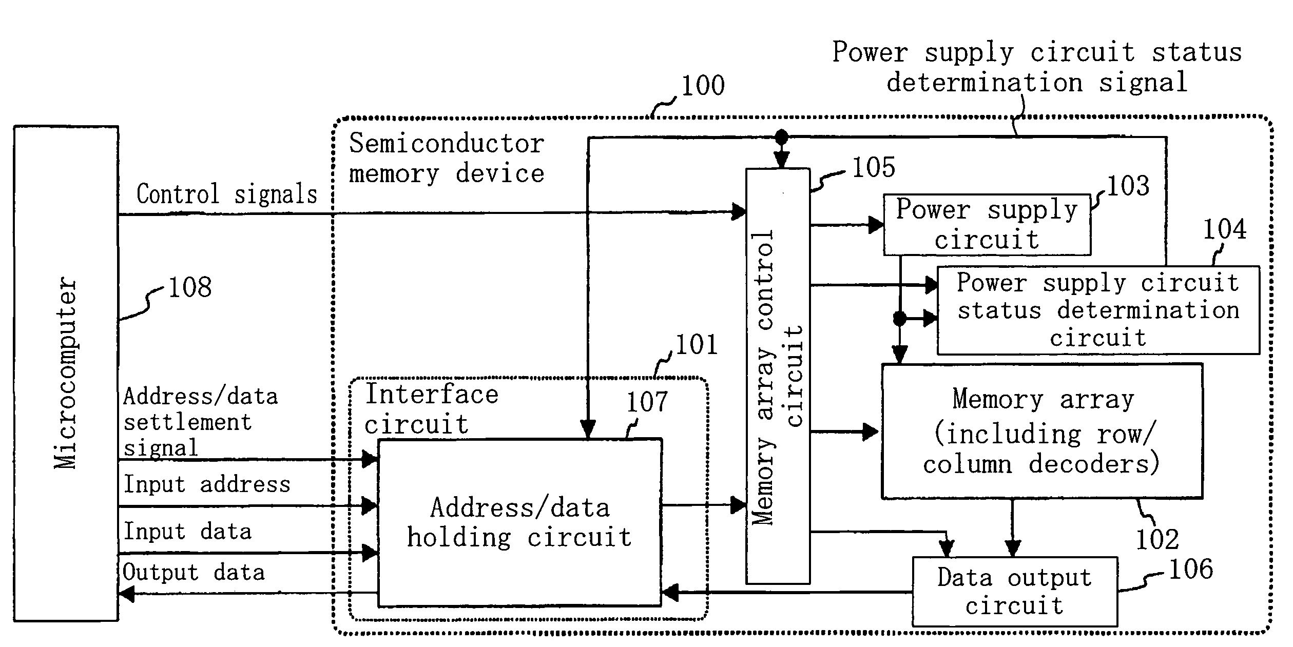
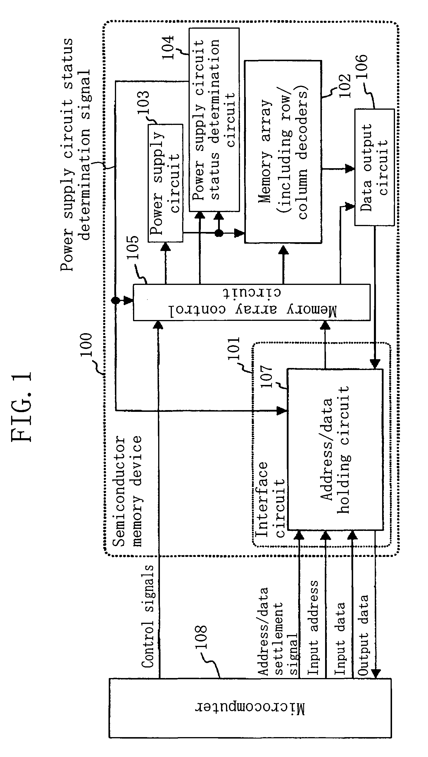
[0033]Referring to FIG. 1, the semiconductor memory device 100 includes an interface circuit 101, a memory array 102, a power supply circuit 103 having a voltage boosting function, a power supply circuit status determination circuit 104, a memory array control circuit 105, and a data output circuit 106.
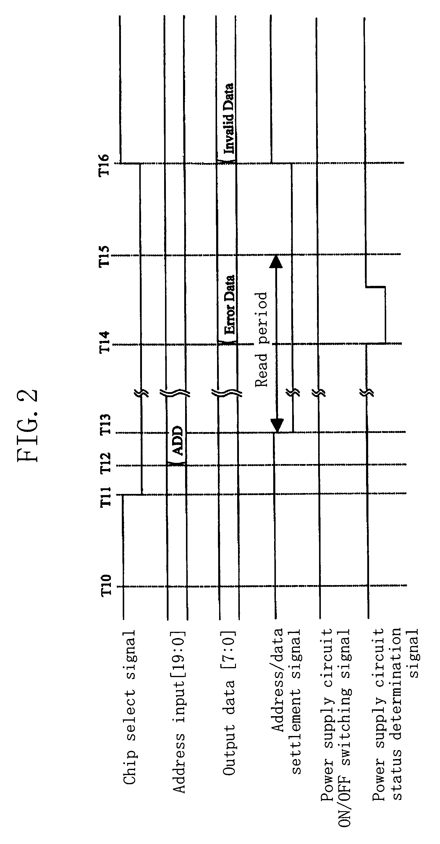
[0034]The semiconductor memory device 100 receives, from a microcomputer 108, a plurality of control signals for controlling the semiconductor memory device 100, an address / data settlement signal, an input address, and input data. The plurality of control signals include a chip select signal, and a power supply circuit ON / OFF switching signal. The semiconductor memory device 100 outputs output data to the microcomputer 108. These signals are exchanged between the semiconductor memory device 100 and the microcomputer 108 in parallel transmission as shown in FIG. 1.
[0035]The chip select signal is a signal for controlling the validity of a read operation, a write operation, or the like o...
embodiment 2
[0050]Referring to FIG. 3, a semiconductor memory device 200 of Embodiment 2 includes an interface circuit 201, a command interpretation circuit 202, the memory array 102, the power supply circuit 103 having a voltage boosting function, the power supply circuit status determination circuit 104, a memory array control circuit 205, and the data output circuit 106. The interface circuit 201 includes a clock counter circuit 203 and an address / data holding circuit 207.
[0051]The semiconductor memory device 200 receives, from a microcomputer 208, a plurality of control signals for controlling the semiconductor memory device 200, a clock signal, an input address, and input data. The plurality of control signals include a chip select signal. The semiconductor memory device 200 outputs output data to the microcomputer 208. In the present embodiment, the input address, the input data and the output data are exchanged between the semiconductor memory device 200 and the microcomputer 208 in seri...
embodiment 3
[0067]Referring to FIG. 5, a semiconductor memory device 300 of Embodiment 3 includes an interface circuit 301, the memory array 102, the power supply circuit 103 having a voltage boosting function, the power supply circuit status determination circuit 104, a memory array control circuit 305, and the data output circuit 106. The interface circuit 301 includes an address / data control circuit 302 and an address / data holding circuit 307.
[0068]The semiconductor memory device 300 receives, from a microcomputer 108, a plurality of control signals for controlling the semiconductor memory device 300, an address / data settlement signal, an input address, and input data. The plurality of control signals include a chip select signal, and a power supply circuit ON / OFF switching signal. The semiconductor memory device 300 outputs output data to the microcomputer 108. These signals are exchanged between the semiconductor memory device 300 and the microcomputer 108 in parallel transmission as shown...
PUM
 Abstract
Description
Claims
Application Information


