CMOS image sensor apparatus with on-chip real-time pipelined JPEG compression module

a technology of image sensor and compression module, which is applied in the field of electromagnetic field, can solve the problems of reducing the video throughput of the system and increasing the cost of the imager modul

Active Publication Date: 2009-05-12
APTINA IMAGING CORP
View PDF31 Cites 24 Cited by
  • Summary
  • Abstract
  • Description
  • Claims
  • Application Information

AI Technical Summary

Problems solved by technology

However, bandwidth limitations imposed by wireless transmission, together with the desire to employ image sensors with large pixel counts, necessitates the use of image compression in the system.
This leads to increased cost of the imager module and reduced video throughput of the system.

Method used


Image

  • CMOS image sensor apparatus with on-chip real-time pipelined JPEG compression module
  • CMOS image sensor apparatus with on-chip real-time pipelined JPEG compression module
  • CMOS image sensor apparatus with on-chip real-time pipelined JPEG compression module

Examples


Embodiment Construction

[0014]In the following detailed description, reference is made to the accompanying drawings that form a part hereof, and in which are shown by way of illustration specific embodiments in which the invention may be practiced. These embodiments are described in sufficient detail to enable those skilled in the art to practice the invention, and it is to be understood that other embodiments may be utilized, and that structural, logical and electrical changes may be made without departing from the spirit and scope of the present invention.

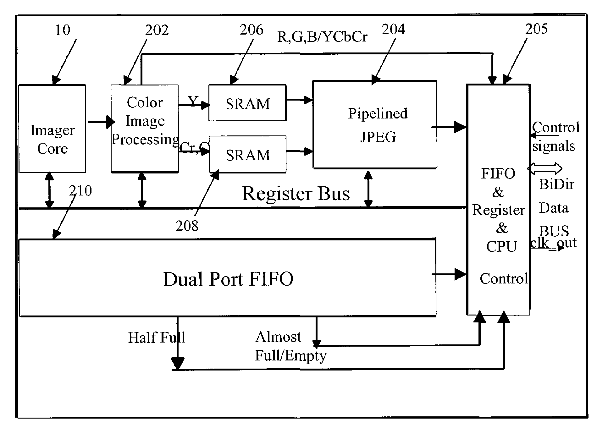
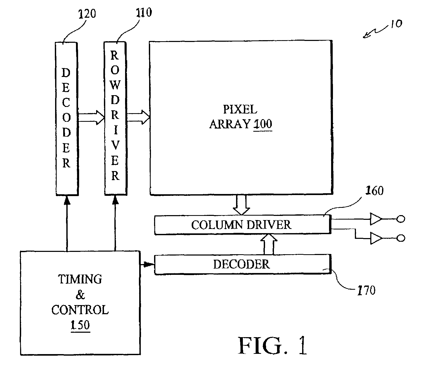
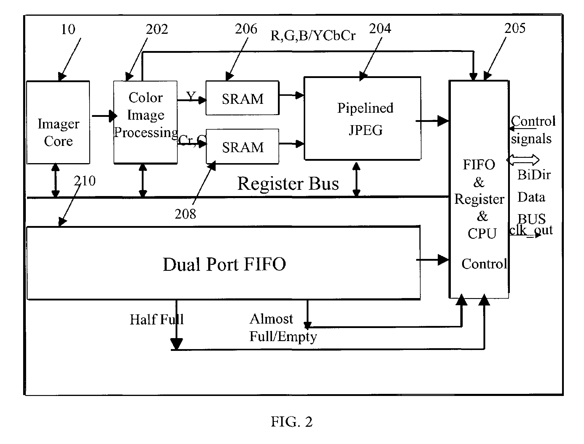
[0015]FIG. 1 illustrates a block diagram for a typical CMOS imager 10 having a pixel array 100 with each pixel cell being constructed in the manner disclosed, for example, in U.S. Pat. No. 6,204,524, the disclosure of which is herein incorporated by reference. Pixel array 100 comprises a plurality of pixels arranged in a predetermined number of columns and rows. The pixels of each row in array 100 are all turned on at the same time by a row select line,...


PUM


Abstract

A CMOS imager in which a CMOS image sensor, a color image processing module and an image compression module are all provided on a single die. Both the color image processing module and the image compression module incorporate pipelined architectures to process the image data at a video rate in a massively parallel fashion.

Description

FIELD OF THE INVENTION[0001]The invention relates generally to improved semiconductor imaging devices and, more specifically, to a CMOS imager provided with an on-chip data compression module.BACKGROUND OF THE INVENTION[0002]A number of different types of semiconductor-based imagers exist, including charge coupled devices (CCDs), CMOS arrays, photodiode arrays, charge injection devices and hybrid focal plane arrays. Recently, however, CMOS imagers have gained popularity in use in a wide variety of electronic devices, because CMOS imagers offer a number of advantages over other types of imagers. CMOS imagers, for example, are compatible with integrated on-chip electronics (control logic and timing, image processing, and signal conditioning such as A / D conversion). CMOS imagers allow random access to the image data. CMOS imagers have lower fabrication costs as compared with the conventional CCD imagers, since standard CMOS processing techniques can be used. Additionally, CMOS imagers ...

Claims


Application Information

Patent Timeline
Patent Type & Authority Patents(United States)
IPC IPC(8): G06K9/20G06K9/28G06K9/36G06K9/46H04N3/14H04N5/335G06T1/20G06V30/144H04N1/41H04N5/374H04N7/26H04N9/07
CPCG06T1/20H04N5/335H04N25/00
Inventor KAPLINSKY, MICHAELSUBBOTIN, IGORLIN, XIUHONG
Owner APTINA IMAGING CORP
Why Eureka
Try Eureka