Method for fabricating CMOS image sensor

a technology of complementary metaloxide semiconductors and image sensors, applied in the field of image sensors, can solve the problems of difficult to keep a shallow depth of boron implantation, limited light efficiency, dark current, etc., and achieve the effects of improving the light efficiency of blue light, small thickness, and reducing crystallization defects

Active Publication Date: 2009-05-26
INTELLECTUAL VENTURES II
View PDF10 Cites 2 Cited by
  • Summary
  • Abstract
  • Description
  • Claims
  • Application Information

AI Technical Summary

Benefits of technology

[0015]It is, therefore, an object of the present invention to provide a complementary metal-oxide semiconductor (CMOS) image sensor, which can improve light efficiency of blue light by forming a P-type impurity region, which is formed to isolate a photodiode and a top surface of a substrate structure, with a small thickness, reduce a crystallization defect, which may occur during an ion implantation process, and improve light characteristics by forming a highly doped P-type impurity region.

Problems solved by technology

However, there are a few limitations while conventionally forming the P-type impurity region 18.
The crystallization defect occurs due to a characteristic of the ion implantation process, that is, ion collision, and the crystallization defect may result in a dark current.
It is difficult to keep a depth of boron implantation shallow due to a characteristic of the ion implantation.
Consequently, the P-type impurity region 18 may not be sufficiently doped, and thus, the P-type impurity region 18 may not function properly, and often results in deteriorated light characteristics.
However, it is difficult to form a highly doped P-type impurity region having a small thickness by employing the BSG deposition method.

Method used


Image

  • Method for fabricating CMOS image sensor
  • Method for fabricating CMOS image sensor
  • Method for fabricating CMOS image sensor

Examples


Embodiment Construction

[0020]A method for fabricating a complementary metal-oxide semiconductor (CMOS) image sensor in accordance with exemplary embodiments of the present invention will be described in detail with reference to the accompanying drawings.

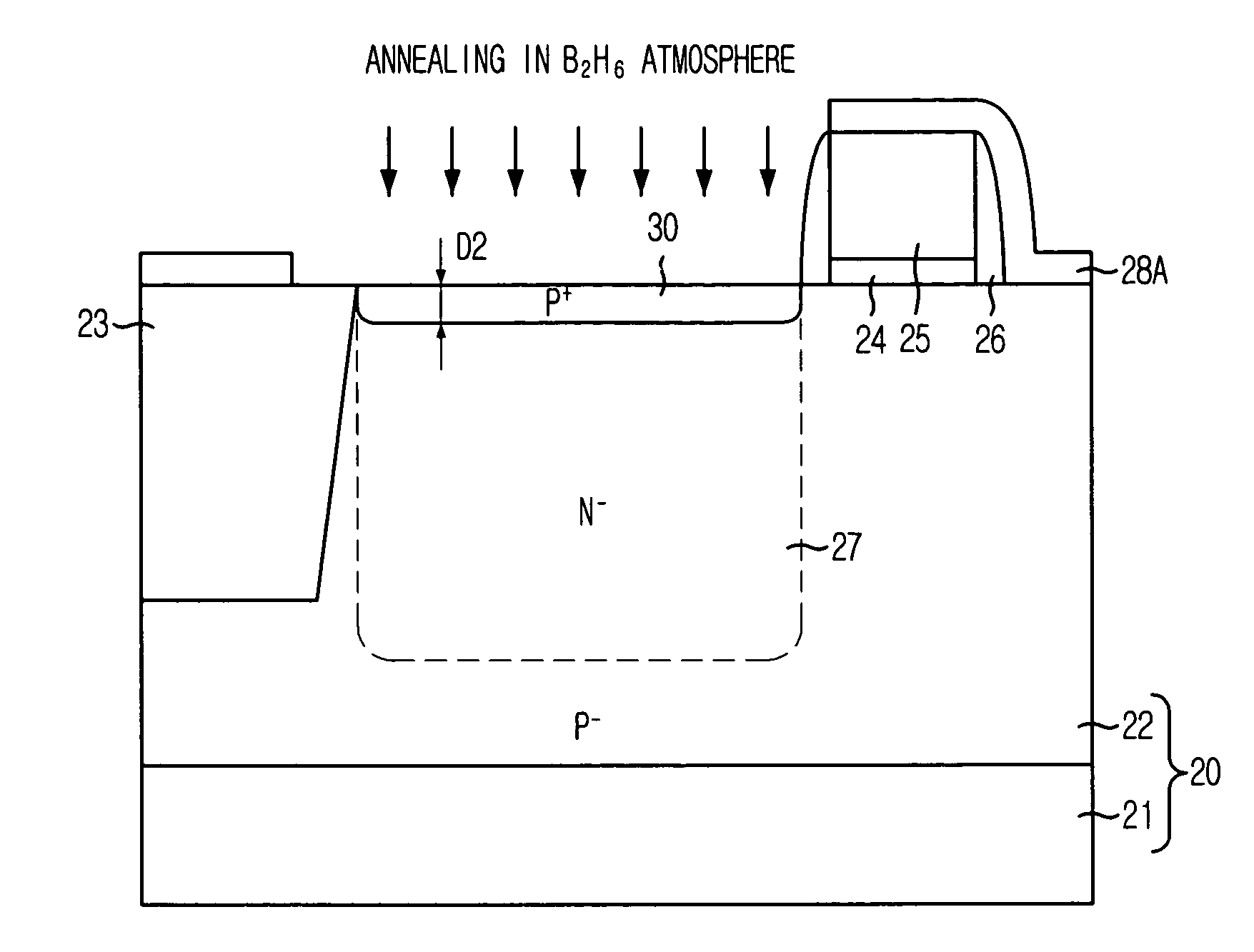
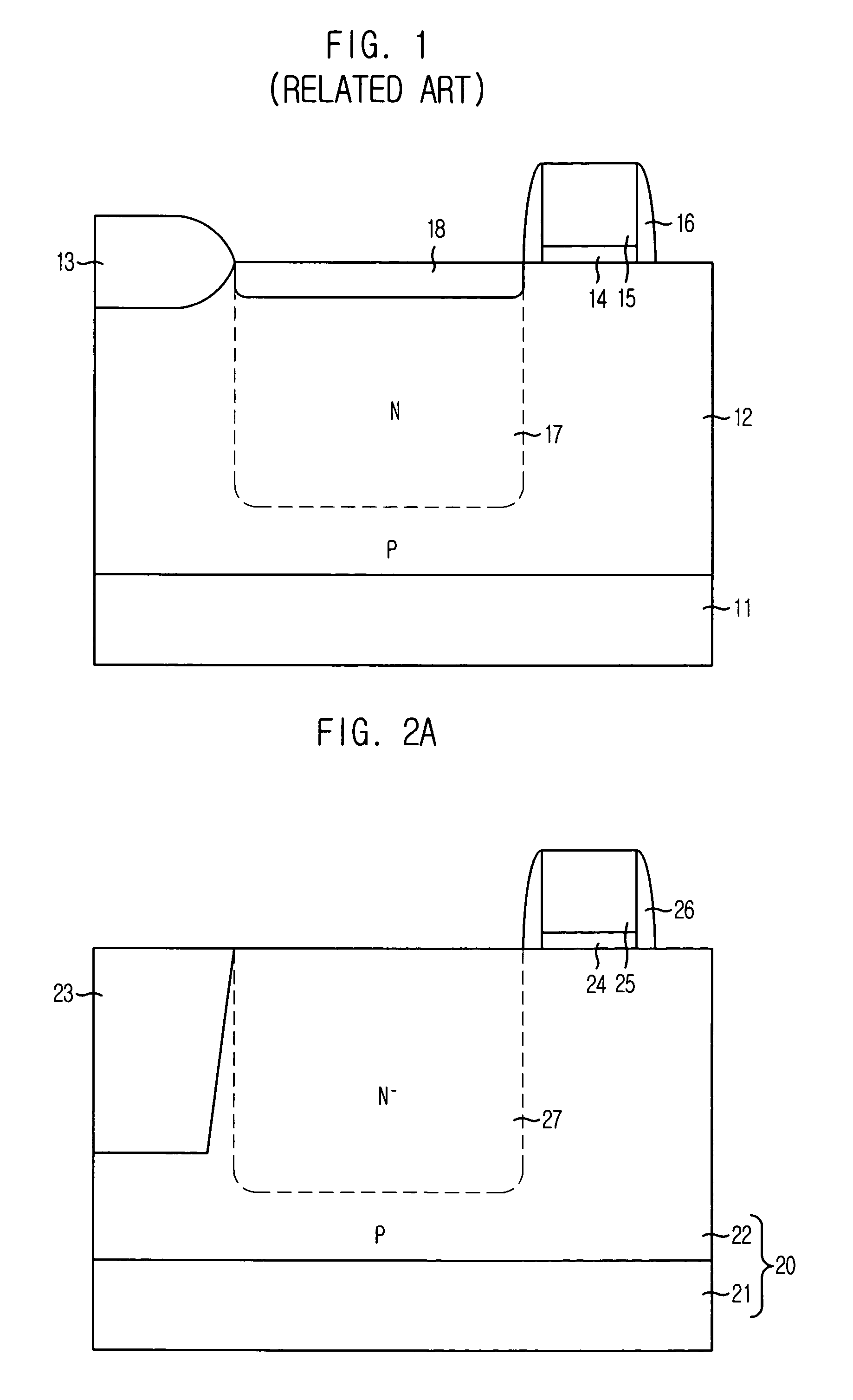
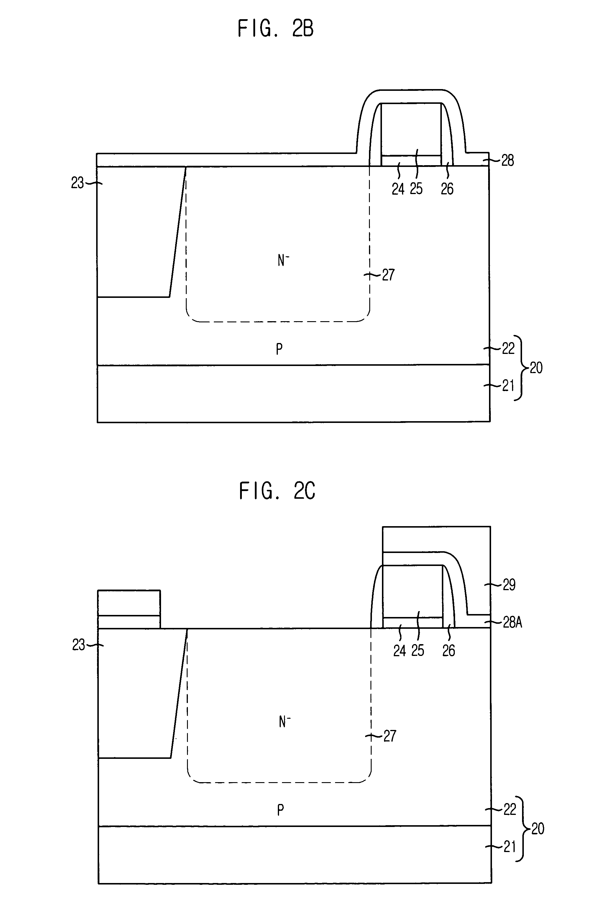
[0021]FIGS. 2A to 2E are cross-sectional views illustrating a method for fabricating a CMOS image sensor in accordance with a specific embodiment of the present invention.

[0022]As shown in FIG. 2A, a P-type epitaxial layer 22 lowly doped with P-type impurities is grown over a P++ substrate 21 highly doped with P-type impurities. A field oxide layer 23 is formed in a predetermined portion of the P-type epitaxial layer 22. Depth of a depletion layer of a photodiode can increase because of the lowly doped P-type epitaxial layer 22, and thus, photosensitivity can be improved. A crosstalk between unit pixels can be reduced by reaggregating the photocharges through the existence of the highly doped P++ substrate 21. The crosstalk occurs due to irregular movement...


PUM


Abstract

A method for fabricating a complementary metal-oxide semiconductor (CMOS) image sensor includes performing an ion implantation process onto a photodiode region in a first conductivity type semiconductor layer to form a second conductivity type first impurity region, and performing an annealing process in a gas atmosphere including first conductivity type impurity atoms to form a first conductivity type second impurity region underneath a surface of the first conductivity type semiconductor layer in the second conductivity type first impurity region, wherein the first conductivity type second impurity region is doped with the diffused first conductivity impurity atoms.

Description

FIELD OF THE INVENTION[0001]The present invention relates to an image sensor, and more particularly, to a method for fabricating a complementary metal-oxide semiconductor (CMOS) image sensor.DESCRIPTION OF RELATED ARTS[0002]Generally, an image sensor is a device that captures image information using a photo-reaction in a semiconductor material. The device transforms electrical values in pixels into a level capable of signalizing, each pixel detecting subjects with different brightness and wavelength. The image sensor generally includes a charge coupled device (CCD) image sensor and a complementary metal-oxide semiconductor (CMOS) image sensor. The image sensor uses a photodiode as a photodetector, which absorbs light captured from an external subject image, and collects and accumulates photocharges.[0003]A typical unit pixel of a CMOS image sensor includes a photodiode and four transistors. The four transistors are a transfer transistor, which transfers photocharges integrated in th...

Claims


Application Information

Patent Timeline
Patent Type & Authority Patents(United States)
IPC IPC(8): H01L21/20
CPCH01L27/14689H01L27/14609H01L27/146
Inventor CHA, HAN-SEOB
Owner INTELLECTUAL VENTURES II
Why Eureka
Try Eureka