Supercharge Your Innovation With Domain-Expert AI Agents!

Image sensor and manufacturing method thereof

a manufacturing method and image sensor technology, applied in the field of image sensors, can solve the problems of low efficiency of image sensors, low quality of image sensors, and inability to form microlens with a complete zero gap, etc., and achieve the effect of improving the characteristics of devices

Active Publication Date: 2009-05-26
III HLDG 4
View PDF5 Cites 0 Cited by
  • Summary
  • Abstract
  • Description
  • Claims
  • Application Information

AI Technical Summary

Benefits of technology

The present invention provides an image sensor and a fabricating method that can prevent the generation of a lens bridge between neighboring pixels of a microlens and form a microlens with a zero gap to improve the characteristics of a device. The image sensor includes a lower structure having a photodiode, a passivation layer, and a microlens array having a first set of microlenses and a second set of microlenses. The fabricating method includes forming a lower structure, a passivation layer, a planarization layer, a photosensitive film, sacrificial microlenses, a first set of microlenses, a second set of microlenses, and a microlens array. The image sensor and the fabricating method can improve image quality and device performance.

Problems solved by technology

These gaps cause the image sensor's performance to suffer.
Accordingly, the minimum gap width is often limited to about 50 nm due to the current limitations of lithography resolution.
Thus, current microlens formation processes cannot form a microlens having a complete zero gap.

Method used


Image

  • Image sensor and manufacturing method thereof
  • Image sensor and manufacturing method thereof
  • Image sensor and manufacturing method thereof

Examples


Embodiment Construction

[0019]When the terms “on” or “over” are used herein, when referring to layers, regions, patterns, or structures, it is understood that the layer, region, pattern or structure can be directly on another layer or structure, or intervening layers, regions, patterns, or structures may also be present. When the terms “under” or “below” are used herein, when referring to layers, regions, patterns, or structures, it is understood that the layer, region, pattern or structure can be directly under the other layer or structure, or intervening layers, regions, patterns, or structures may also be present.

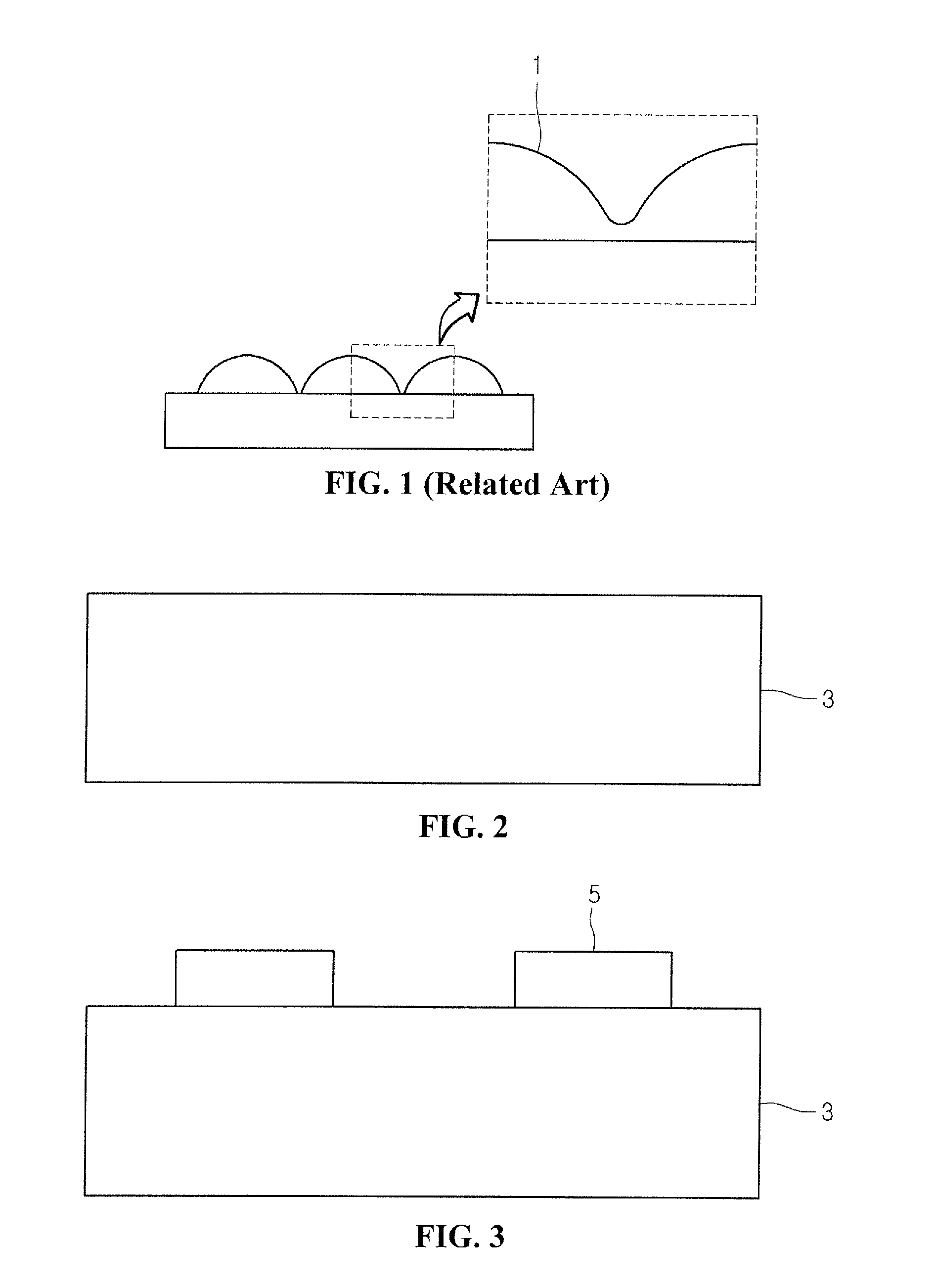
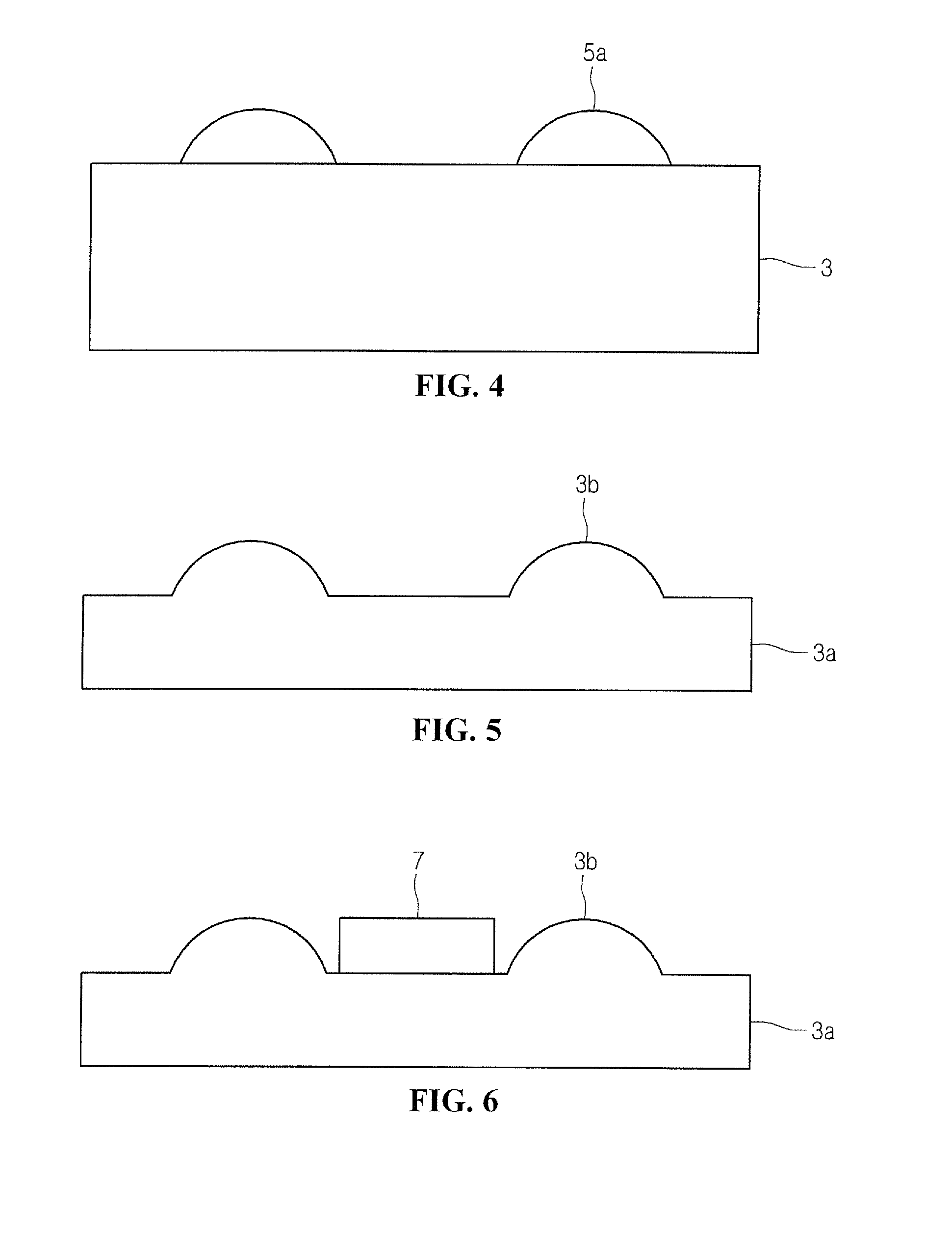
[0020]Referring to FIG. 2, in an embodiment of the fabricating method of the present invention, a lower layer 3 is formed before forming a microlens (ML) pattern. The lower layer 3 can be etched by means of a dry etching method, such as reactive ion etching (RIE). In many embodiments, the lower layer 3 is formed of a hydrophilic material.

[0021]In certain embodiments, the lower layer 3 serves as...


PUM

PropertyMeasurementUnit
gap widthaaaaaaaaaa
temperatureaaaaaaaaaa
RIaaaaaaaaaa

Abstract

An image sensor and method for fabricating an image sensor are provided. The image sensor includes a substrate and a microlens array in a checkerboard pattern. In some embodiments, the checkerboard pattern involves alternating hydrophilic and hydrophobic microlenses.

Description

CROSS-REFERENCE TO RELATED APPLICATION[0001]The present application claims the benefit under 35 U.S.C. § 119 of Korean Patent Application No. 10-2006-0135715, filed on Dec. 27, 2006, and Korean Patent Application No. 10-2006-0135716, filed on Dec. 27, 2006, which are each hereby incorporated by reference in their entirety.BACKGROUND[0002]An image sensor is a semiconductor device that converts an optical image into an electrical signal. The fabrication process is very important in determining the performance of an image sensor. Two important processes are the color filter array (CFA) and microlens (ML) formation processes.[0003]In a microlens formation process, there are typically gaps formed between neighboring microlenses. These gaps cause the image sensor's performance to suffer. Several studies and simulations have demonstrated that when the gaps are small, the photo sensitivity of the image sensor can be improved by more than 15%.[0004]A typical microlens formation process in th...

Claims


Application Information

Patent Timeline
Patent Type & Authority Patents(United States)
IPC IPC(8): G02B27/10B29D11/00
CPCB29D11/00365G02B3/0018G02B3/0056H01L27/14627H01L27/14685
Inventor YUN, YOUNG JEPARK, JIN HO
Owner III HLDG 4
Features
  • R&D
  • Intellectual Property
  • Life Sciences
  • Materials
  • Tech Scout
  • Unparalleled Data Quality
  • Higher Quality Content
  • 60% Fewer Hallucinations
Learn More