Integrated ring modulator array WDM transceiver

a ring modulator array and transceiver technology, applied in the field of optical transceivers, can solve the problems of large gap between the i/o bandwidth density required on the electronic chip versus, limit the capacity of optical transceivers, and electrical i/o on the off-chip side, etc., to achieve the effect of facilitating optical multiplexing and demultiplexing

Active Publication Date: 2009-05-26
ORACLE INT CORP
View PDF5 Cites 26 Cited by
  • Summary
  • Abstract
  • Description
  • Claims
  • Application Information

AI Technical Summary

Benefits of technology

[0012]One embodiment of the present invention provides a system that facilitates optical multiplexing and demultiplexing. The system includes an optical transmitter which is structured in the following way. A wavelength-splitting mechanism is coupled to the optical transmitter, which separates the wavelengths of light onto an array of input-optical-waveguide busses within the optical transmitter. An array of ring modulators within the optical transmitter is coupled to each optical-waveguide bus, whe...

Problems solved by technology

One factor that limits the capacity of optical transceivers, and hence the communication capacity between electronic components within the system, is the total number of lasers or optical modulators that can be integrated into the transceiver package.
In high-end systems applications, a large gap exists between the I/O bandwidth density required on an electronic chip versus what present-day optical interconnect technology is capable of delivering.
Although significant advances in off-chip electrical I/O and signaling density have been achieved for short transmission lengths, off-chip electrical I/O has many disadvantages, including high electrical power dissipation and limited transmission length (approximately one meter).
Unfortunately, existing optical technology cannot meet the bandwidth requirements in a package comparable to the size of the chip.
However, existing optical solutions can only achieve 10-100 times smaller bandwidth onto such a chip.
Another limitation of the existing ...

Method used


Image

  • Integrated ring modulator array WDM transceiver
  • Integrated ring modulator array WDM transceiver
  • Integrated ring modulator array WDM transceiver

Examples


Embodiment Construction

[0035]The following description is presented to enable any person skilled in the art to make and use the invention, and is provided in the context of a particular application and its requirements. Various modifications to the disclosed embodiments will be readily apparent to those skilled in the art, and the general principles defined herein may be applied to other embodiments and applications without departing from the spirit and scope of the present invention. Thus, the present invention is not limited to the embodiments shown, but is to be accorded the widest scope consistent with the principles and features disclosed herein.

Integrated WDM Transceiver

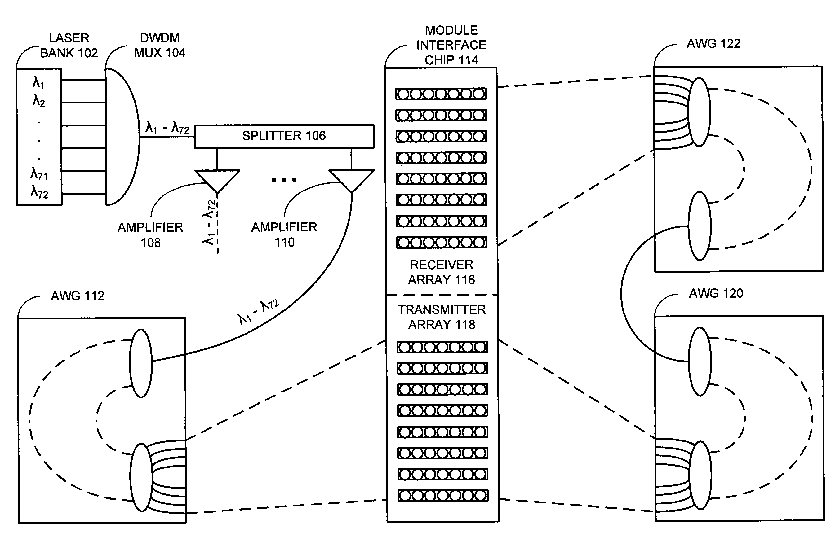
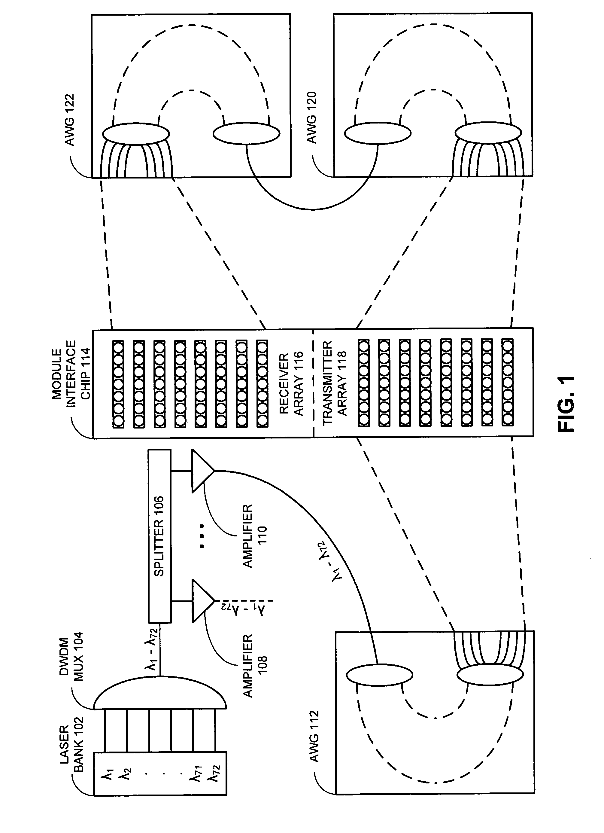
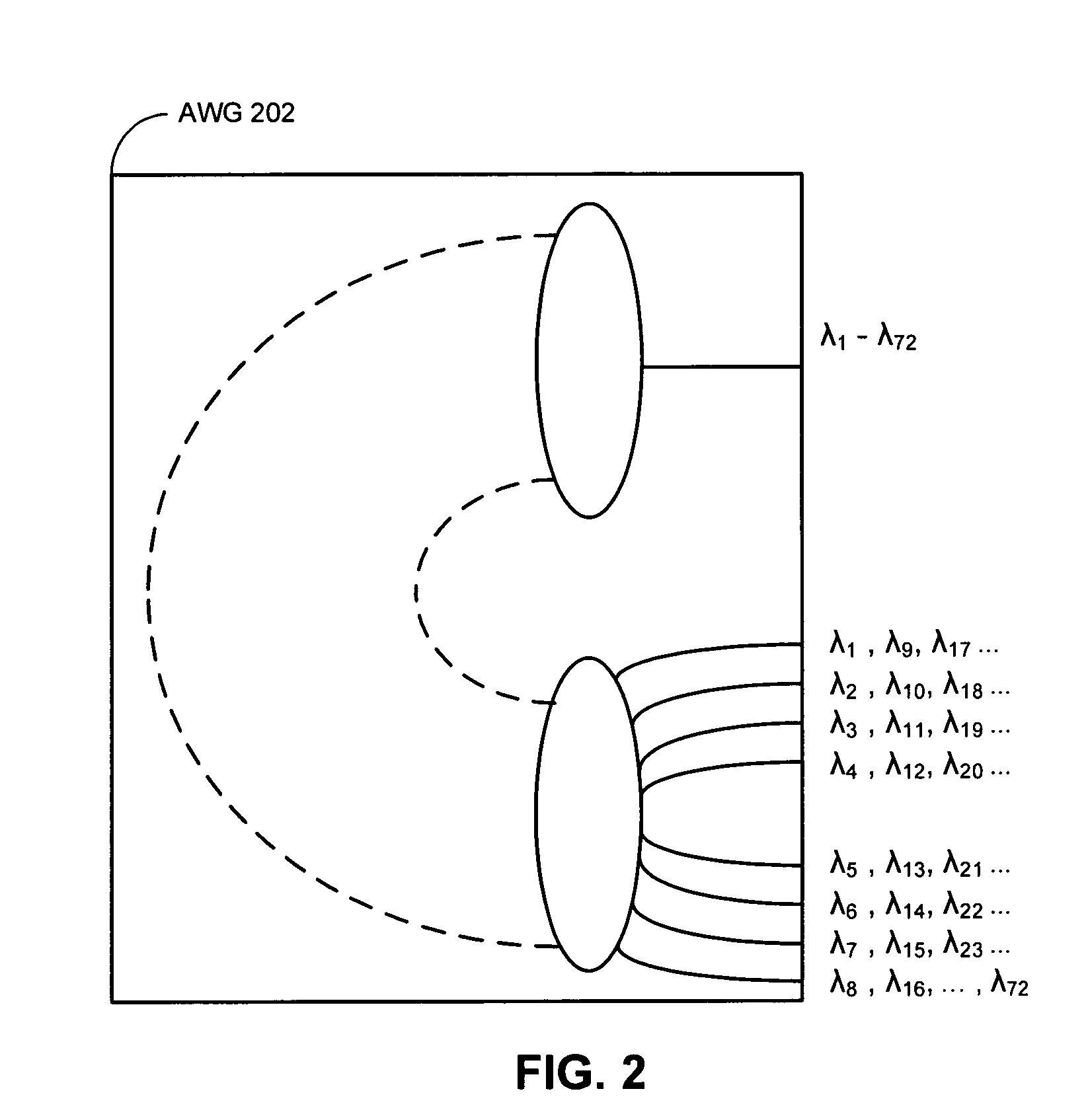
[0036]The present invention provides efficient structures and techniques for constructing dense, parallel optical transceivers with large aggregate bandwidths. These optical transceivers contain many parallel channels that can scale to an aggregate capacity of multiple terabits-per-second and beyond. In one embodiment of the present ...


PUM


Abstract

A system that facilitates optical multiplexing and demultiplexing. The system includes an optical transmitter which is structured in the following way. A wavelength-splitting mechanism is coupled to the optical transmitter, which separates the wavelengths of light onto an array of input-optical-waveguide busses within the optical transmitter. An array of ring modulators within the optical transmitter is coupled to each optical-waveguide bus, wherein the input-end of a given ring modulator is coupled to a corresponding input-optical-waveguide bus. Output-optical-waveguide busses within the optical transmitter are coupled to the array of ring modulators, wherein the output-end of each ring modulator is coupled to a corresponding output-optical-waveguide bus. When a modulation signal is applied to a given ring modulator within the array of ring modulators, a specific wavelength of light is directed to the corresponding output-optical-waveguide bus.

Description

BACKGROUND[0001]1. Field of the Invention[0002]The present invention relates to the design of optical transceivers. More specifically, the present invention relates to a multi-dimensional wavelength-division-multiplexing (WDM) transceiver that permits multiple WDM transceivers to be co-located on a single semiconductor chip.[0003]2. Related Art[0004]Optical transceivers convert high-speed electrical signals into optical signals (and vice-versa) for transmission through fiber optic cables. Optical transceivers are also commonly used for communicating data between electronic components within a datacenter. These optical transceivers populate the boards and cards within a data communications or telecommunications chassis, and communicate to other chips within the chassis.[0005]One factor that limits the capacity of optical transceivers, and hence the communication capacity between electronic components within the system, is the total number of lasers or optical modulators that can be i...

Claims


Application Information

Patent Timeline
IPC IPC(8): H04J14/02H04B10/00
CPCG02F1/011H04J14/02G02F2201/16G02F2203/05G02F2203/15
Inventor KRISHNAMOORTHY, ASHOK V.CUNNINGHAM, JOHN E.
Owner ORACLE INT CORP
Why Eureka
Try Eureka