Signal receiver apparatus and method for detecting logic state represented by an input signal and semiconductor integrated circuit device having the same
- Summary
- Abstract
- Description
- Claims
- Application Information
AI Technical Summary
Benefits of technology
Problems solved by technology
Method used
Image

Examples
Embodiment Construction
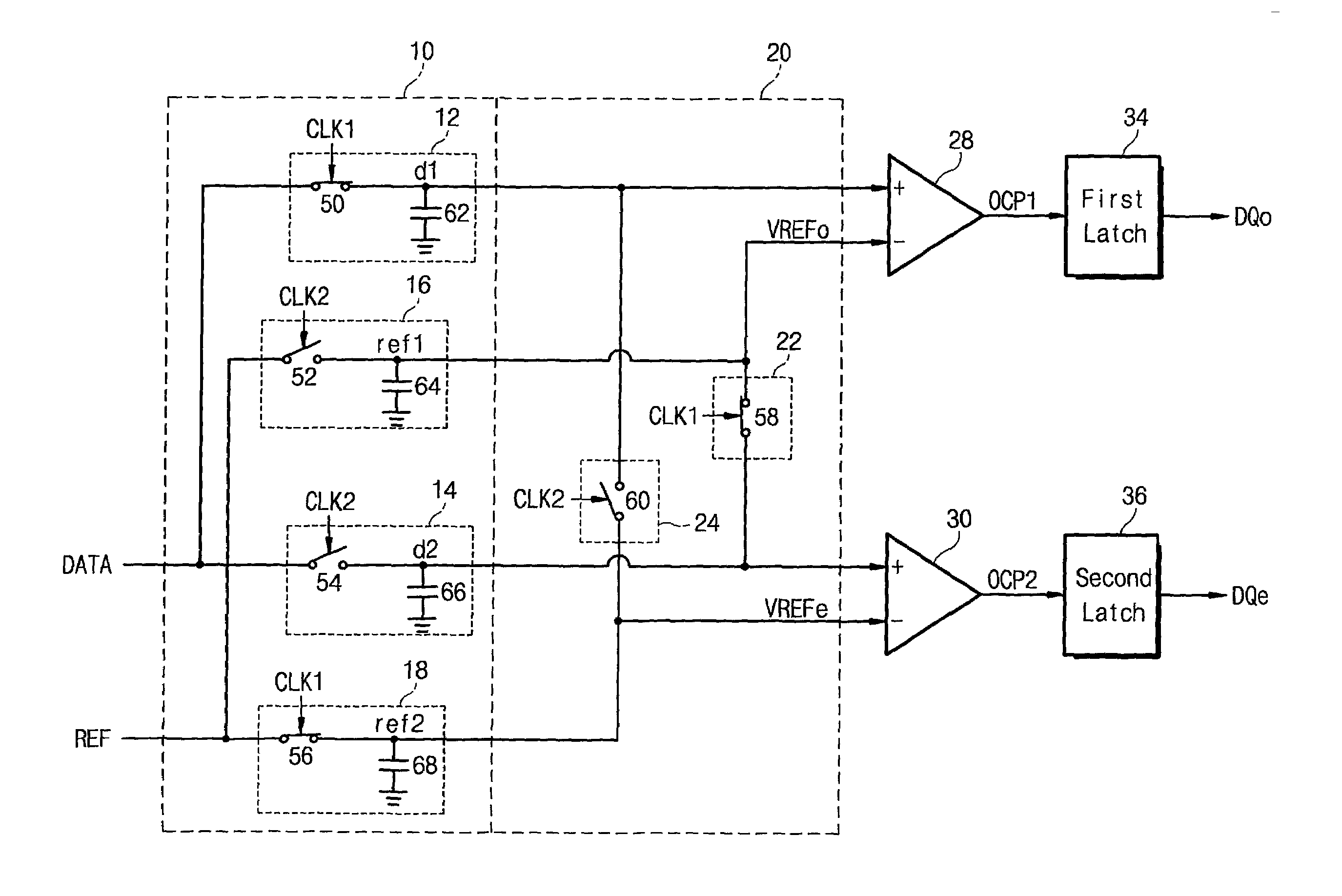
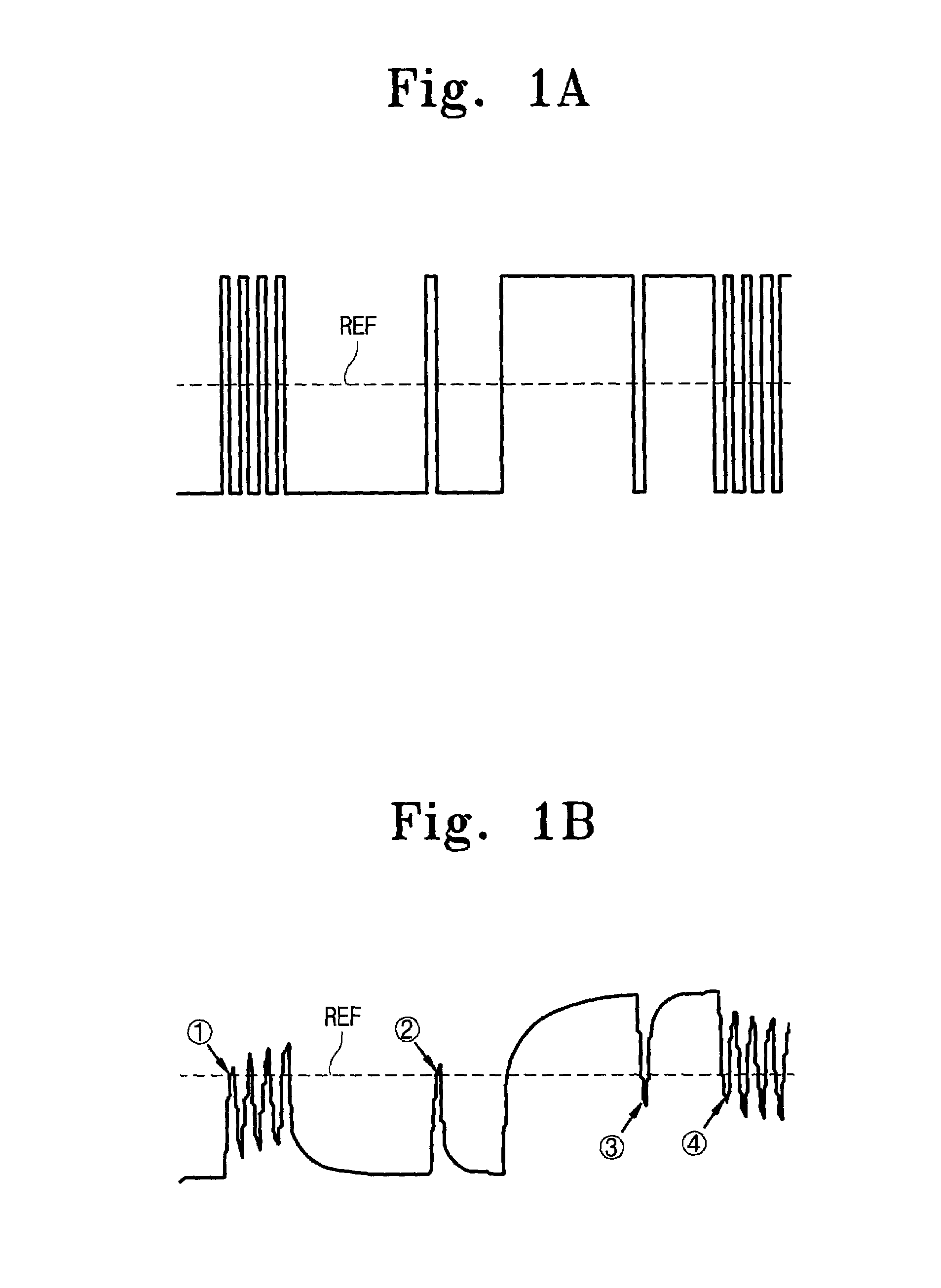
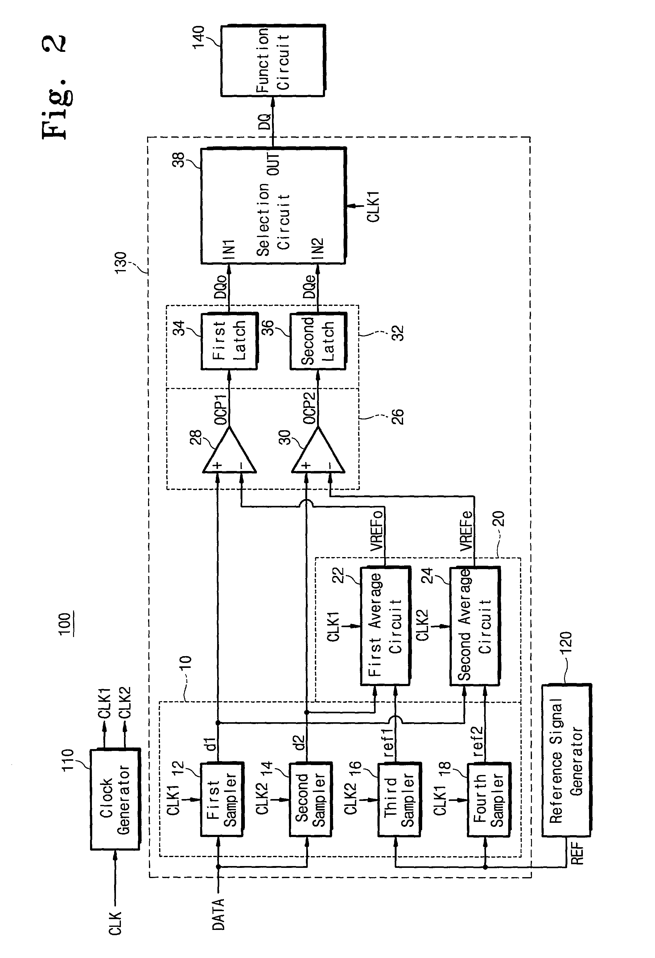
[0017]FIG. 2 is a block diagram, which schematically illustrates a circuit configuration of an embodiment of a signal receiver apparatus according to the present invention, and FIG. 3 is a waveform diagram for explaining a logic level identification technique according to the invention.
[0018]Referring to FIG. 2, a signal receiver apparatus 100 includes a clock generator 110 that is synchronized with a clock signal CLK externally provided (hereinafter referred to as “external clock signal”) to internally generate first and second clock signals CLK1 and CLK2 (hereinafter referred to as “first and second internal clock signals CLK1 and CLK2”). The first and second internal clock signals CLK1 and CLK2 are complementary signals having phases opposite to each other, as shown in FIG. 4. Alternatively, the receiver apparatus 100 may receive clock signals CLK1 and CLK2 from the exterior. In this case, the receiver apparatus 100 does not need the clock generator 110.
[0019]The receiver apparat...
PUM
 Abstract
Description
Claims
Application Information
 - R&D Engineer
- R&D Manager
- IP Professional
- Industry Leading Data Capabilities
- Powerful AI technology
- Patent DNA Extraction
Browse by: Latest US Patents, China's latest patents, Technical Efficacy Thesaurus, Application Domain, Technology Topic.
© 2024 PatSnap. All rights reserved.Legal|Privacy policy|Modern Slavery Act Transparency Statement|Sitemap