
Segmented bitscan for verification of programming

a bitcan and programming technology, applied in the field of nonvolatile storage, can solve the problems of consuming substantial time and power, slow cell program or erase, and inability to program or erase cells, etc., and achieve the effect of more error bits and more error bits

Active Publication Date: 2009-06-09
SANDISK TECH LLC
View PDF30 Cites 10 Cited by
  • Summary
  • Abstract
  • Description
  • Claims
  • Application Information

AI Technical Summary

Benefits of technology

The patent proposes a system for tolerating more errors in a non-volatile memory system. The system groups data into overlapping zones, with each zone spanning multiple sectors. During programming, the system checks each zone to determine if it has fewer errors than the maximum correctable for a sector. This allows for more errors to be tolerated. The system also includes a control circuit that determines if there are fewer errors in overlapping groups of non-volatile storage elements. The technical effect is to improve the reliability and accuracy of non-volatile memory systems.

Problems solved by technology

Of course, a tradeoff exists between the yield savings and the cost of providing additional memory cells to store the code bits (i.e., the code “rate”).
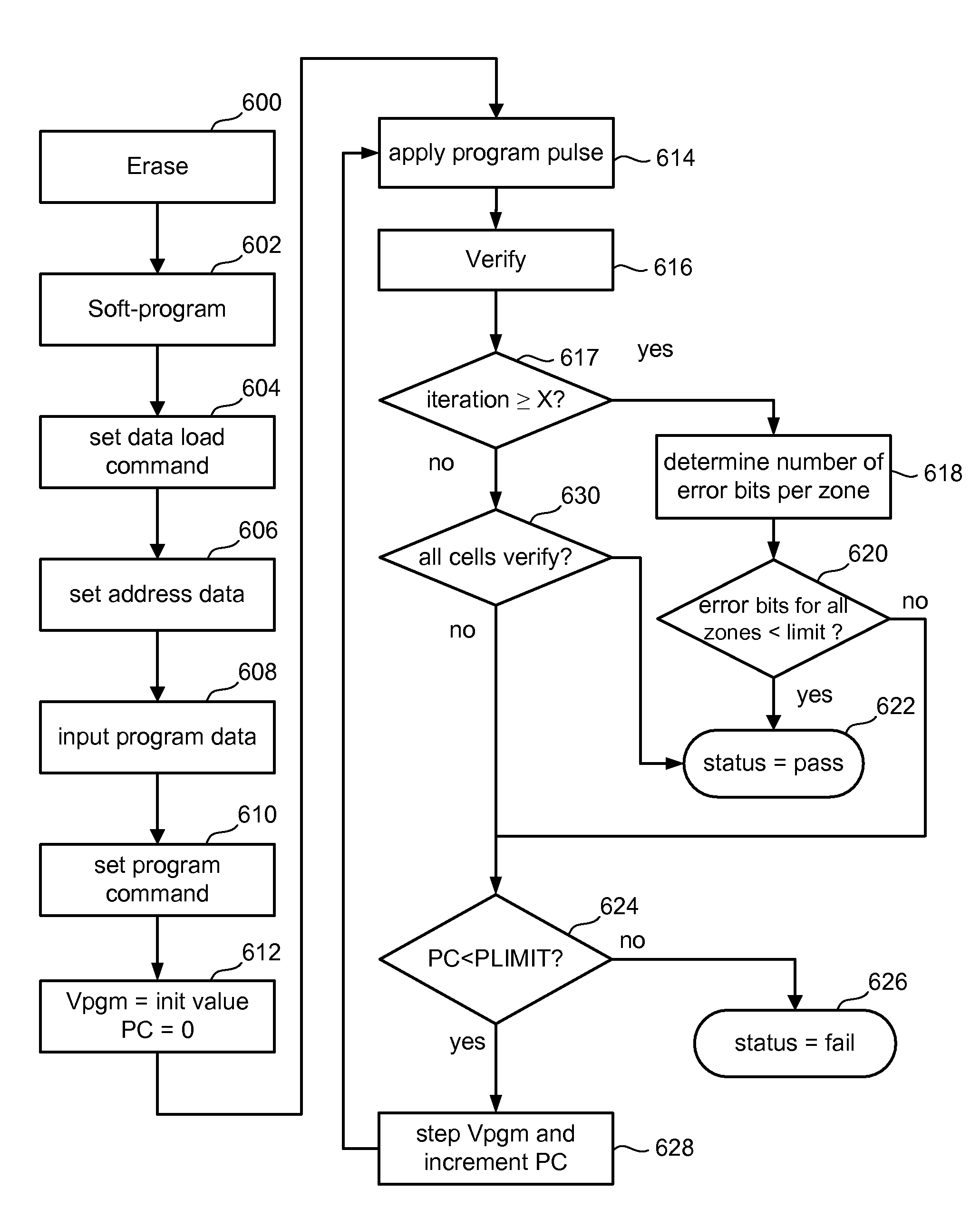
Indeed, considering that the programming and erasing of flash memory cells are typically performed by the application of a sequence of pulses of the appropriate voltages, and also considering that the pulse sequences consume substantial time and power, many flash memories now include verification operations during the programming or erasing operations themselves.
As is well known in this art, some memory cells are slower to program or erase than others, because of manufacturing variations among those cells, because those cells were previously erased to a lower threshold voltage than others, because of uneven wear among the cells within a page, or the like.
And, of course, some cells cannot be programmed or erased whatsoever, because of a defect or other reason.
However, in conventional circuitry, the verification process counts errors (bits that have not properly programmed) across the entire page, regardless of the position of the error bit.
The typical system described above will not conclude that programming was successful, despite the ability of ECC to correct one error per sector.

Method used


Image

  • Segmented bitscan for verification of programming
  • Segmented bitscan for verification of programming
  • Segmented bitscan for verification of programming

Examples


Embodiment Construction

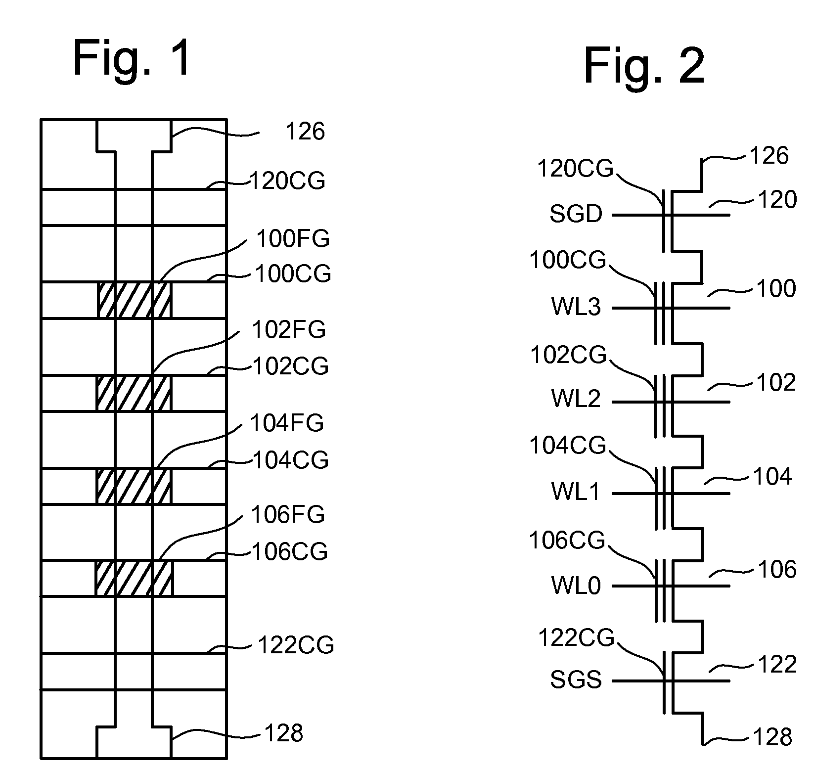
[0050]One example of a memory system suitable for implementing the present invention uses the NAND flash memory structure. However, other types of non-volatile storage devices can also be used. For example, a so called TANOS structure (consisting of a stacked layer of TaN—Al2O3—SiN—SiO2 on a silicon substrate), which is basically a memory cell using trapping of charge in a nitride layer (instead of a floating gate), can also be used with the present invention. Another type of memory cell useful in flash EEPROM systems utilizes a non-conductive dielectric material in place of a conductive floating gate to store charge in a non-volatile manner. Such a cell is described in an article by Chan et al., “A True Single-Transistor Oxide-Nitride-Oxide EEPROM Device,” IEEE Electron Device Letters, Vol. EDL-8, No. 3, March 1987, pp. 93-95. A triple layer dielectric formed of silicon oxide, silicon nitride and silicon oxide (“ONO”) is sandwiched between a conductive control gate and a surface of...


PUM


Abstract

A set non-volatile storage elements are subjected to a programming process in order to store a set of data. During the programming process, one or more verification operations are performed to determine whether the non-volatile storage elements have reached their target condition to store the appropriate data. Decisions about whether to continue programming or whether the programming is successful are made based on whether overlapping groups of the non-volatile storage elements have less than a threshold number of non-volatile storage elements that are not properly programmed.

Description

CROSS-REFERENCE TO RELATED APPLICATIONS[0001]The following application is cross-referenced and incorporated by reference herein in its entirety: U.S. patent application Ser. No. 11 / 563,590, entitled “Apparatus With Segmented Bitscan For Verification Of Programming,” by Yan Li, Teruhiko Kamei and Jeffrey Lutze, filed Nov. 27, 2006, now U.S. Pat. No. 7,440,319.BACKGROUND OF THE INVENTION[0002]1. Field of the Invention[0003]The present invention relates to technology for non-volatile storage.[0004]2. Description of the Related Art[0005]Semiconductor memory devices have become more popular for use in various electronic devices. For example, non-volatile semiconductor memory is used in cellular telephones, digital cameras, personal digital assistants, mobile computing devices, non-mobile computing devices and other devices. Electrical Erasable Programmable Read Only Memory (EEPROM) and flash memory are among the most popular non-volatile semiconductor memories.[0006]Many types of EEPROM ...

Claims


Application Information

Patent Timeline
Patent Type & Authority Patents(United States)
IPC IPC(8): G11C16/04
CPCG11C11/5628G11C16/0483G11C16/3454G11C2211/5621
Inventor LI, YANKAMEI, TERUHIKOLUTZE, JEFFREY W.
Owner SANDISK TECH LLC
Learn More