Method for fabricating semiconductor device, and electro-optical device, integrated circuit and electronic apparatus including the semiconductor device

a semiconductor and substrate technology, applied in the field of pattern formation exposure technique, can solve the problems of reducing affecting the quality so as to reduce the cost, enhance and reduce the resolution of the exposed image.

Inactive Publication Date: 2009-06-16
SEIKO EPSON CORP
View PDF20 Cites 209 Cited by
  • Summary
  • Abstract
  • Description
  • Claims
  • Application Information

AI Technical Summary

Benefits of technology

[0005]In terms of cost reduction, uneven substrates, such as inexpensive glass substrates, are used for fabrication of electro-optical devices, such as liquid crystal displays. It is, however, difficult to expose a pattern on such an uneven substrate at a high resolution. If accurate projection exposure is sought at a reduced cost using a stepper or a scanner, considering the margin of error which is encountered in volume production, the resolution of the exposed image is necessarily compromised. In particular, it can become more difficult to enhance the resolution of the exposed image when large display devices are produced. In contrast, with the holographic exposure technique, theoretically no optical aberration is present so that it readily enhances the resolution of the exposed image. This holographic exposure technique, however, has the drawback of a lower throughput as compared to related art or known exposure methods using, e.g., a stepper. Therefore, repeated use of holography enhances the resolution of the exposed image, but reduces the productivity of volume production. In this respect, in the related art, it is difficult to simultaneously achieve high-resolution exposure and volume production when forming a pattern on an uneven substrate.
[0006]The present invention provides a technique that enables formation of minute patterns on an uneven substrate in volume production without reducing productivity.

Problems solved by technology

It is, however, difficult to expose a pattern on such an uneven substrate at a high resolution.
If accurate projection exposure is sought at a reduced cost using a stepper or a scanner, considering the margin of error which is encountered in volume production, the resolution of the exposed image is necessarily compromised.
In particular, it can become more difficult to enhance the resolution of the exposed image when large display devices are produced.
This holographic exposure technique, however, has the drawback of a lower throughput as compared to related art or known exposure methods using, e.g., a stepper.
Therefore, repeated use of holography enhances the resolution of the exposed image, but reduces the productivity of volume production.
In this respect, in the related art, it is difficult to simultaneously achieve high-resolution exposure and volume production when forming a pattern on an uneven substrate.

Method used


Image

  • Method for fabricating semiconductor device, and electro-optical device, integrated circuit and electronic apparatus including the semiconductor device
  • Method for fabricating semiconductor device, and electro-optical device, integrated circuit and electronic apparatus including the semiconductor device
  • Method for fabricating semiconductor device, and electro-optical device, integrated circuit and electronic apparatus including the semiconductor device

Examples


Embodiment Construction

[0027]Exemplary embodiments of the present invention are described with reference to the drawings. First, an exposure method according to the present invention is briefly described.

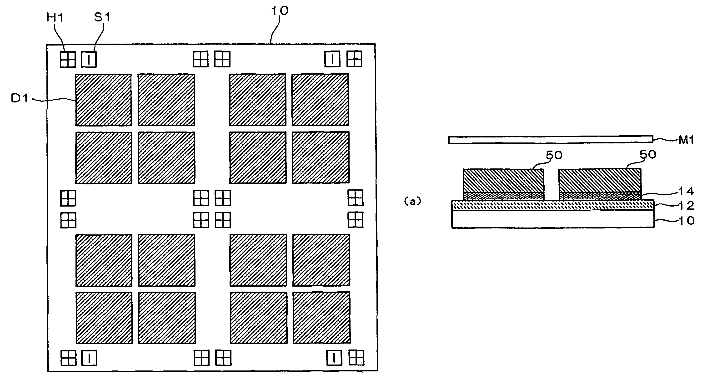
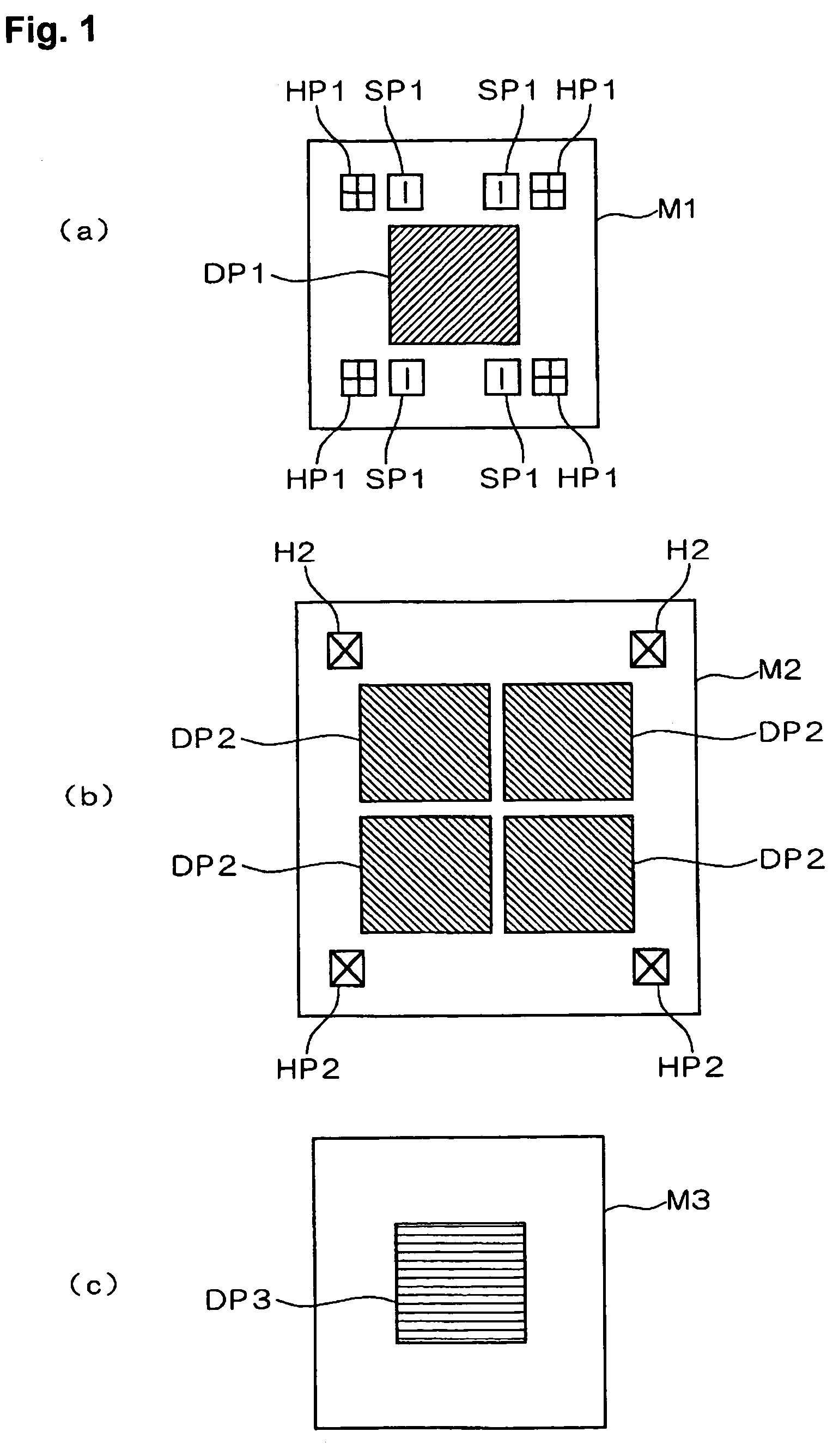
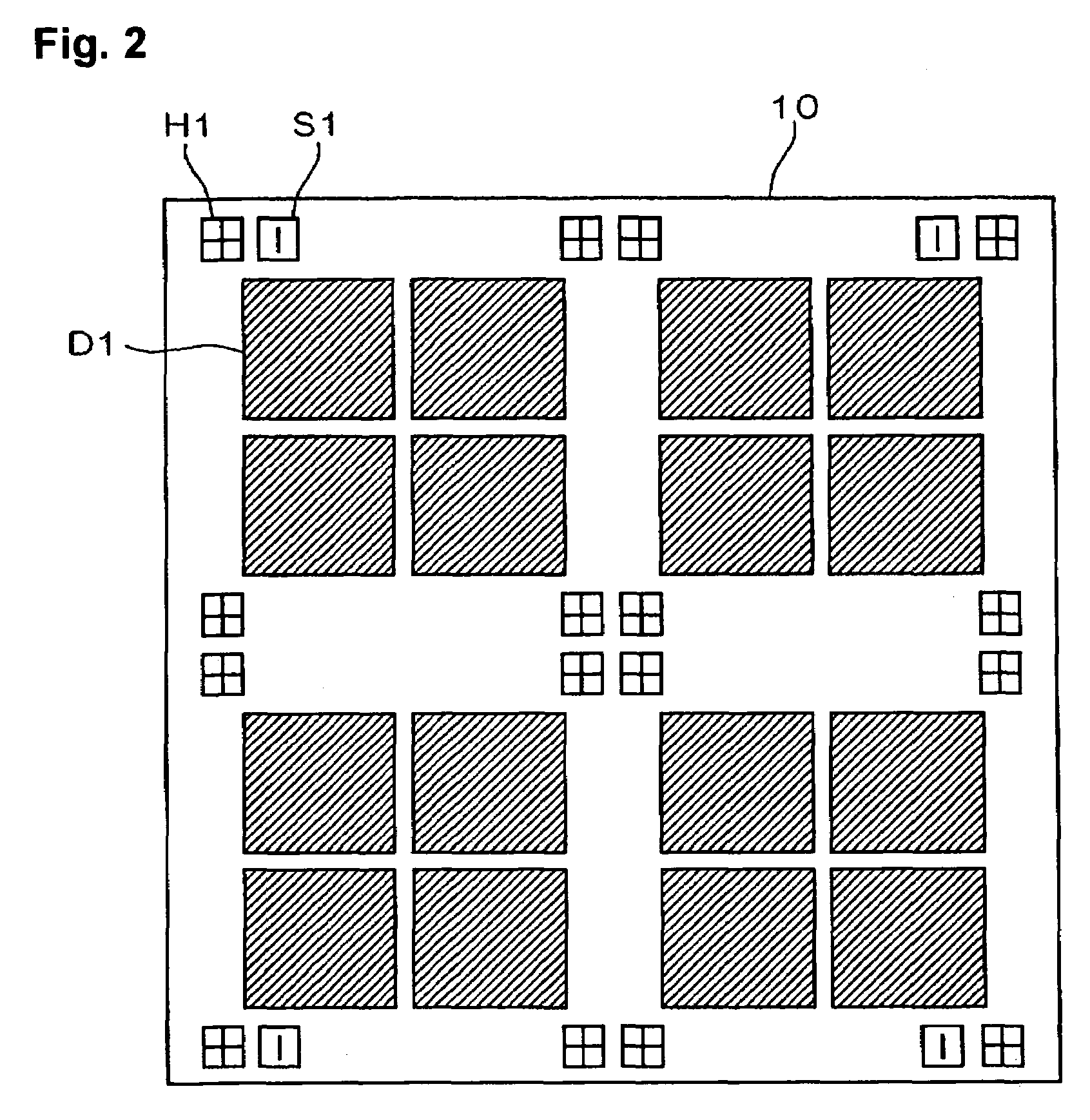
[0028]FIGS. 1(a)-1(c) are schematics describing exposure masks used in a method for fabricating a semiconductor device according to the present invention. In this exemplary embodiment, a process of fabricating semiconductor devices which include thin film elements, such as thin film transistors, is described. Exposure is performed at least three times in the process. Among the three exposures, the first and third exposures are conducted using a projection exposure system, such as a stepper or a scanner, and the second exposure is conducted using a holographic exposure system. FIG. 1(a) illustrates an exposure mask or a reticle M1 used for the first projection exposure. FIG. 1(b) illustrates an exposure mask or holographic mask M2 used for the second holographic exposure. FIG. 1(c) illustrates an exposure ...


PUM

PropertyMeasurementUnit
gate lengthaaaaaaaaaa
temperatureaaaaaaaaaa
thicknessaaaaaaaaaa

Abstract

The invention provides a technique that enables formation of minute patterns on an uneven substrate in volume production without reducing productivity. The method for fabricating a semiconductor device includes: first patterning a semiconductor film on a substrate to form element regions, each of which will be provided with a source / drain region and a channel region, second forming a gate insulating film covering segments of the patterned semiconductor film in the respective element regions, third forming gate electrodes on the gate insulating film at predetermined positions, and fourth forming the source / drain region and the channel region in each element region. At least the gate electrodes are formed by a process including an exposure step through a holographic exposure mask in the third step, and by a process including an exposure step through a projection exposure mask, the element regions are formed in the first step, and the source / drain regions and the channel regions are formed in the fourth step.

Description

BACKGROUND OF THE INVENTION[0001]1. Field of Invention[0002]The present invention relates to a method for fabricating a semiconductor device, such as a thin film transistor. More particularly, the invention relates to an exposure technique for pattern formation.[0003]2. Description of Related Art[0004]Processes of fabricating semiconductor devices, such as thin film transistors, use exposure techniques in order to print desired patterns on substrates. Holographic exposure techniques can be beneficial since they offer high-resolution exposure. An example of the holographic exposure techniques is described in Francis Clube et al., “Large-field, high-resolution photolithography”, Proc. SPIE 1997, Vol. 3099, pp. 36-45.SUMMARY OF THE INVENTION[0005]In terms of cost reduction, uneven substrates, such as inexpensive glass substrates, are used for fabrication of electro-optical devices, such as liquid crystal displays. It is, however, difficult to expose a pattern on such an uneven substrat...

Claims


Application Information

Patent Timeline
Patent Type & Authority Patents(United States)
IPC IPC(8): H01L21/00G03F1/42G03F7/22G03F9/00H01L21/027H01L21/28H01L21/336H01L21/77H01L21/84H01L27/12H01L29/786
CPCH01L27/1214H01L27/1288B42D15/045B42D15/08
Inventor IRIGUCHI, CHIHARU
Owner SEIKO EPSON CORP
Why Eureka
Try Eureka