Superlattice strain relief layer for semiconductor devices

a technology of superlattice strain relief and semiconductor devices, which is applied in the direction of semiconductor lasers, lasers, solid-state devices, etc., can solve the problems of lower operating voltage due to the vertical device structure, and achieve the effects of low defect, high aluminum content, and low operating voltag

Active Publication Date: 2009-06-16
XEROX CORP
View PDF19 Cites 125 Cited by
  • Summary
  • Abstract
  • Description
  • Claims
  • Application Information

AI Technical Summary

Benefits of technology

[0013]Accordingly, the present invention is directed to a GaN / AlN strain relief layer that enables the growth of crack-free thick AlGaN films with high aluminum content on a GaN / sapphire template. According to one aspect of the present invention, an ultraviolet InAlGaN light emitting diode heterostructure is grown on a GaN / sapphire template with a GaN / AlN short period superlattice (SPSL) strain relief layer. The short period superlattice strain relief layer enables the growth of a high-quality and crack-free high aluminum content InAlGaN MQWH active region, providing a light emitting diode capable of emitting in the deep UV wavelength range. The GaN / AlN short period superlattice strain relief layer may be formed in conditions (e.g., temperature and pressure) consistent with the growth of other layers of the device for efficient production.
[0014]Optionally, after growth, the deep UV light emitting diode may be flip-chip bonded onto a heatsink and the sapphire substrate removed by excimer laser lift-off. The absorbing GaN template layer and some or all of the GaN / AlN short period superlattice strain relief layer may also be removed, for example by dry-etching (e.g. by CAlBE). Removal of the GaN / sapphire template allows for improved light extraction through the UV-transparent AlGaN current spreading layer and results also in lower operating voltages due to the vertical device structure.
[0015]According to another embodiment of the present invention, a GaN / AlN strain relief layer enables the growth of low defect, relatively high Al-content films over a GaN / sapphire template useful for non-optical applications, such as the high electron mobility transistors (HEMTs) and the like.

Problems solved by technology

Removal of the GaN / sapphire template allows for improved light extraction through the UV-transparent AlGaN current spreading layer and results also in lower operating voltages due to the vertical device structure.

Method used


Image

  • Superlattice strain relief layer for semiconductor devices
  • Superlattice strain relief layer for semiconductor devices
  • Superlattice strain relief layer for semiconductor devices

Examples


Embodiment Construction

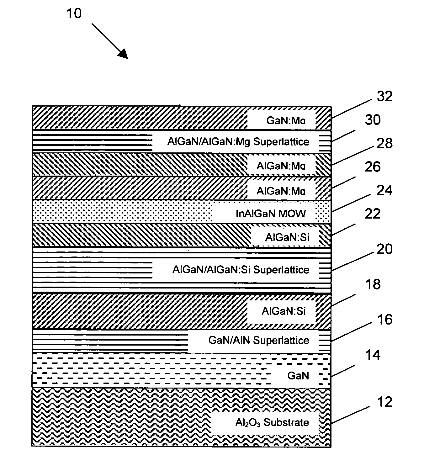
[0025]With reference now to FIG. 1, there is shown therein an index guided, buried heterostructure AlGaInN light emitting diode structure in accordance with the present invention. Diode structure comprises an Al2O3 (sapphire) substrate 12 on which is formed a 2-10 micron thick epitaxial GaN template layer 14. GaN template layer 14 can be Si-doped or undoped and is typically grown at approximately 1100 degree C. and a reactor pressure of approximately 200 Torr. Formed thereon is a GaN / AlN superlattice layer 16, described further below. Formed next is AlGaN:Si. buffer layer 18, and formed thereon is AlGaN / AlGaN:Si superlattice n-strain layer 20 which allows for increased cladding thickness and hence reduced optical leakage of subsequent layers. Formed next is AlGaN:Si n-cladding (index guiding) layer 22. InAlGaN multiple quantum well active layer 24 is formed on layer 22. Formed thereon is AlGaN:Mg p-cladding (index guiding) layer 26, then AlGaN:Mg buffer layer 28. AlGaN / AlGaN:Mg p-st...


PUM


Abstract

A GaN / AlN superlattice is formed over a GaN / sapphire template structure, serving in part as a strain relief layer for growth of subsequent layers (e.g., deep UV light emitting diodes). The GaN / AlN superlattice mitigates the strain between a GaN / sapphire template and a multiple quantum well heterostructure active region, allowing the use of high Al mole fraction in the active region, and therefore emission in the deep UV wavelengths.

Description

CROSS-REFERENCE TO RELATED APPLICATIONS[0001]The present invention is related to provisional U.S. Applications for Letters Patent titled “Superlattice Strain Relief Layer For Semiconductor Devices”, U.S. Ser. No. 60 / 736,362, and “Method For Controlling The Structure And Surface Qualities Of A Thin Film And Product Produced Thereby”, U.S. Ser. No. 60 / 736,531, each filed on Nov. 14, 2005, each assigned to the same assignee as the present application, to which priority is hereby claimed, and each being incorporated by reference herein.STATEMENT REGARDING FEDERALLY SPONSORED RESEARCH AND DEVELOPMENT[0002]The U.S. Government has a fully paid-up license in this invention and the right in limited circumstances to require the patent owner(s) to license others on reasonable terms as provided for by the terms of contract number N66001-02-C-8017 awarded by the Defense Advanced Research Projects Agency, and contract number DAAH01-03-9-R003 sponsored by the U.S. Army Aviation and Missile Command...

Claims


Application Information

Patent Timeline
Patent Type & Authority Patents(United States)
IPC IPC(8): H01L27/15H01L33/04H01L33/32
CPCB82Y20/00H01L29/155H01L29/205H01L33/04H01L29/2003H01L33/32H01S5/0213H01S5/0216H01S5/0217H01S5/0224H01S5/34333H01S5/0234
Inventor WONG, WILLIAM S.KNEISSL, MICHAEL A.YANG, ZHIHONGTEEPE, MARKKNOLLENBERG, CLIFF
Owner XEROX CORP
Why Eureka
Try Eureka