SRAM cell

a technology of sram cells and sram cells, applied in the direction of semiconductor devices, semiconductor/solid-state device details, electrical apparatus, etc., can solve the problem of partially depleting channels, and achieve the effect of greater current carrying capacity and greater effective widths

Inactive Publication Date: 2009-06-16
INT BUSINESS MASCH CORP
View PDF17 Cites 33 Cited by
  • Summary
  • Abstract
  • Description
  • Claims
  • Application Information

AI Technical Summary

Benefits of technology

[0010]Furthermore, the gates of the pull-down FETs are longer than the gates (i.e., the first gates and the second gates, respectively) of the pass-gate and pull-up FETs. Specifically, the pull-down FET gates have a predetermined length that is necessary to achieve a predetermined channel width-to-gate length ratio that is sufficient to suppress short-channel effects and to increase the drive current of the pull-down transistor relative to that of the pass-gate transistor and the pull-up transistor.
[0016]After forming the semiconductor fins, gates (i.e., first gates, second gates and third gates) can be formed adjacent the corresponding fins. If the pass-gate and pull-up FETs are formed as finFETs, then gates (i.e., first and second gates, respectively) are formed on the opposing sidewalls of the first and second semiconductor fins. If the pass-gate and pull-up FETs are formed as trigate FETs, the gates (i.e., first and second gates, respectively) are formed on the opposing sidewalls and top surfaces of the first and second semiconductor fin. Additionally, regardless of whether the pass-gate and pull-up FETs are finFETs or trigate FETs, at least three gates (i.e., third gates) are formed adjacent the top surface and opposing sidewalls of the third semiconductor fins. The third gates are formed longer than the first gates and the second gates and with a predetermined fin (or channel) width-to-gate length ratio so as suppress short-channel effects caused by the partial depletion and to increase a drive current of the pull-down FETs relative to that of the pass-gate and pull-up FETs.
[0017]Once the gates are formed, additional processing may include forming source / drain extensions, forming halos, forming spacers, forming source / drain regions, depositing and planarizing a blanket dielectric layer, forming contacts to the gates, etc. Additionally, if the SRAM cell is formed with either a bulk wafer or a hybrid orientation wafer and p-wells are formed below the channel of the pull-down n-FETs, then contacts can also be formed to the p-wells so that an electrical bias can be applied to the p-wells in order to further control the threshold voltages of the pull-down n-FETs and to further suppress short-channel effects.

Problems solved by technology

Specifically, the pull-down FET channels have a predetermined width necessary to achieve a predetermined height-to-width ratio that results in the channel being partially depleted.

Method used


Image

  • SRAM cell
  • SRAM cell
  • SRAM cell

Examples


Embodiment Construction

[0028]The embodiments of the invention and the various features and advantageous details thereof are explained more fully with reference to the non-limiting embodiments that are illustrated in the accompanying drawings and detailed in the following description. It should be noted that the features illustrated in the drawings are not necessarily drawn to scale. Descriptions of well-known components and processing techniques are omitted so as to not unnecessarily obscure the embodiments of the invention. The examples used herein are intended merely to facilitate an understanding of ways in which the embodiments of the invention may be practiced and to further enable those of skill in the art to practice the embodiments of the invention. Accordingly, the examples should not be construed as limiting the scope of the invention.

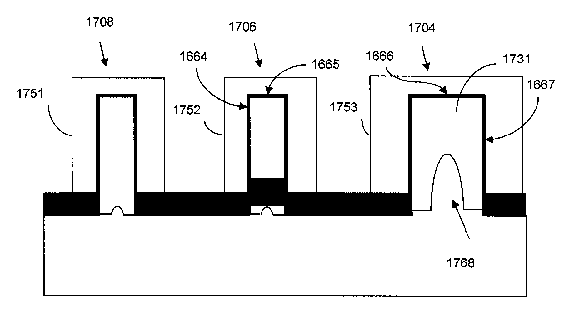
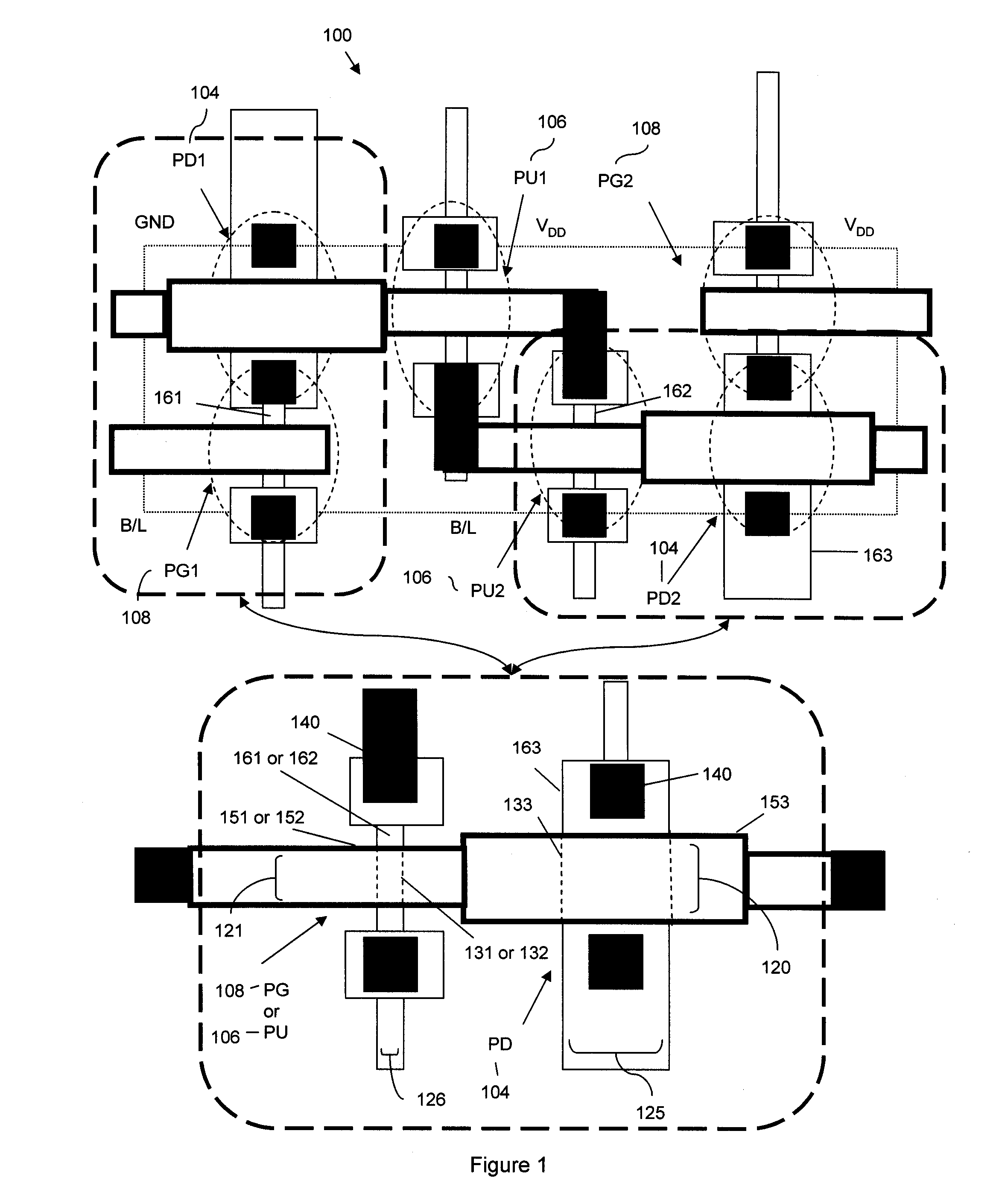
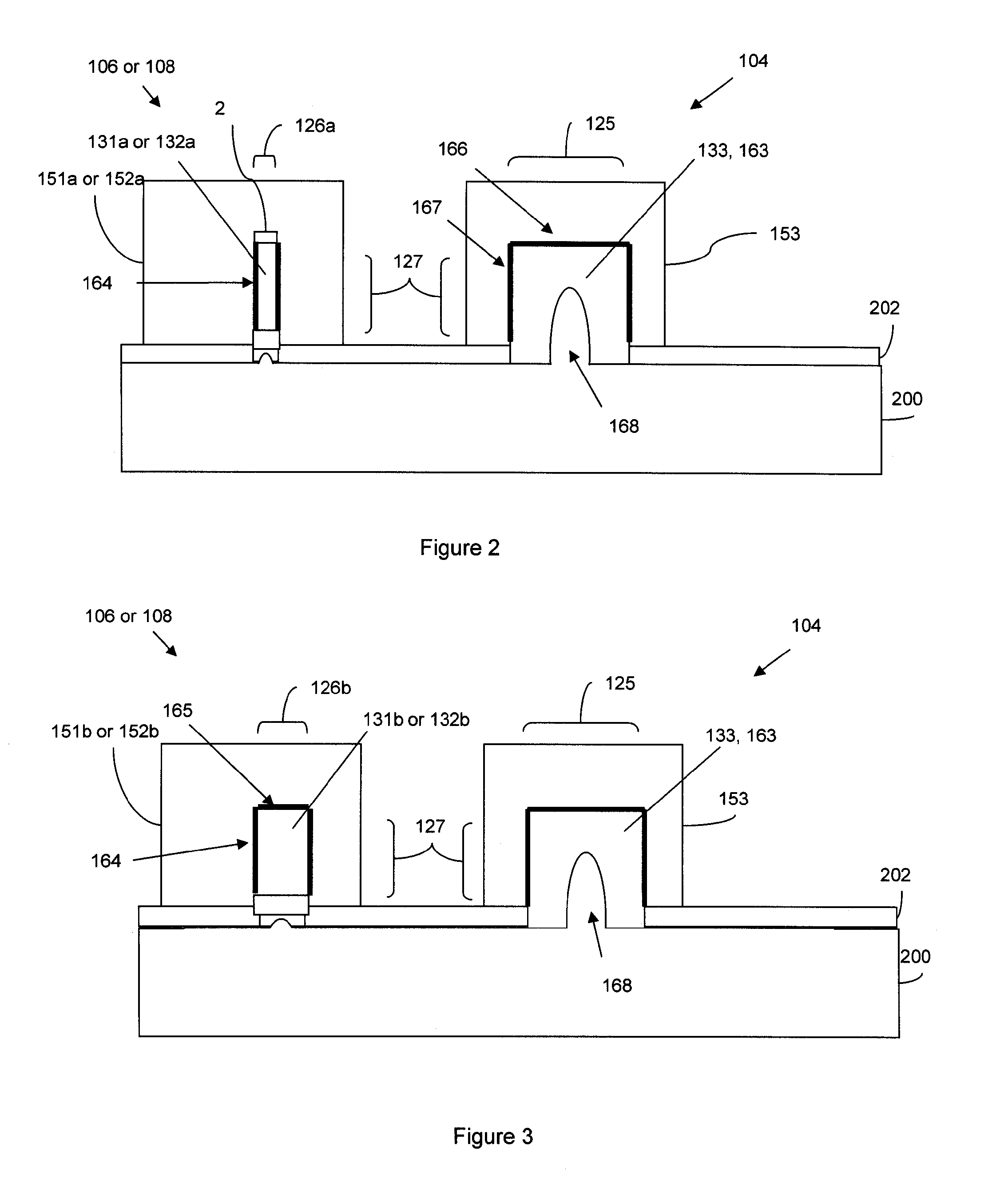
[0029]As mentioned above, due to the conventional lithographic techniques used to pattern fins for non-planar SRAM cells (regardless of the type of wafer used, e.g...


PUM


Abstract

Disclosed is an SRAM cell on an SOI, bulk or HOT wafer with two pass-gate n-FETs, two pull-up p-FETs and two pull-down n-FETs and the associated methods of making the SRAM cell. The pass-gate FETs and pull-down FETs are non-planar fully depleted finFETs or trigate FETs. The pull-down FETs comprise non-planar partially depleted three-gated FETs having a greater channel width and a greater gate length and, thus, a greater drive current relative to the pass-gate and pull-up FETs. Additionally, for optimal electron mobility and hole mobility, respectively, the channels of the n-FETs and p-FETs can comprise semiconductors with different crystalline orientations.

Description

BACKGROUND OF THE INVENTION[0001]1. Field of the Invention[0002]The invention generally relates to the field of semiconductor integrated circuit design and, more particularly, to non-planar static random access memory (SRAM) cell design.[0003]2. Description of the Related Art[0004]Integrated circuit design decisions are often driven by device scalability and manufacturing efficiency. For example, size reduction of single-gate planar metal oxide semiconductor field effect transistors (MOSFETs) often results in reduced drive current because the width of the device is associated with the drive. In response, multi-gated non-planar transistors, such as double-gated FETs (e.g., fin-type FETs (finFETs)) or trigate FETs, were developed to provide scaled devices with faster drive currents and reduced short channel effects.[0005]FinFETs are non-planar transistors in which a fully depleted channel region is formed in the center of a thin semiconductor fin with source and drain regions in the o...

Claims


Application Information

Patent Timeline
Patent Type & Authority Patents(United States)
IPC IPC(8): H01L21/00H01L23/62H01L29/10
CPCH01L27/11H01L27/1104H01L29/785H01L2924/0002Y10S257/903H01L2924/00H10B10/00H10B10/12
Inventor ANDERSON, BRENT A.NOWAK, EDWARD J.
Owner INT BUSINESS MASCH CORP
Why Eureka
Try Eureka