Method for separating semiconductor substrate

a technology of semiconductor substrate and separation method, which is applied in the direction of manufacturing tools, welding/soldering/cutting articles, solid-state devices, etc., can solve the problems of substrate method, loss of cutting portion, and loss of blade width, so as to prevent the loss of substrate, prevent the defective implementation of semiconductor chips, and reduce the force required for separation

Inactive Publication Date: 2009-06-23
DENSO CORP
View PDF14 Cites 30 Cited by
  • Summary
  • Abstract
  • Description
  • Claims
  • Application Information

AI Technical Summary

Benefits of technology

[0013]In this manner, the implementation member is fittingly cut into a suitable size for the semiconductor chip, and defective implementation of the semiconductor chip is prevented. Further, the separation method with a formation of the modified area by the laser beam prevents the loss of the substrate caused by the width of the dicing blade and / or by chipping of the substrate in the course of separation.
[0014]The separation method in the present invention forms the modified area in the substrate along the separation line to be used as a partial cut of the substrate. Therefore, the thickness of the substrate at the partial cut becomes thinner than the other portion of the substrate, and irradiation time of the laser beam for separating the substrate becomes shorter than a standard time. Further, the force required for the separation becomes smaller.
[0015]The separation method in the present invention irradiates the laser beam from either one of the two surfaces of the substrate. Further, two laser beams may be irradiated at the same time from one source of the laser beam onto both sides of the substrate. In this manner, the substrate does not have to be flipped to receive the laser beam from both sides in the course of separation. Further, a laser beam irradiation system may be simplified when a single source of the laser beam generates two laser beams for the separation process, and thereby having a decreased production cost, a decreased maintenance cost and a decreased failure rate. Furthermore, the separation time is decreased when two layers of modified areas along the separation line are formed by two laser beams at the same time.

Problems solved by technology

The separation method of the substrate suffers from problems such as a loss of cutting portion, that is, a blade width lost in the course of cutting, and a chipping of the substrate that deteriorates a yield rate of the substrate.
In this case, the strength of implementation will decrease because of an insufficient space of adhesion when the DAF 2b has a size that is smaller than a standard size.
In addition, the implementation will be defective when a residue DAF 2c extending from the semiconductor chip 1e (shown in FIG. 4C) prevents a normal implementation.
The semiconductor chip 1e suffers from a same type of problem when the implementation of the chip 1e by soldering with a metal foil is substituted for the implementation by using the DAF.
That is, it is problematic in the implementation of the semiconductor chip when the DAF or the metal foil is not suitably cut with the semiconductor chip.

Method used


Image

  • Method for separating semiconductor substrate
  • Method for separating semiconductor substrate
  • Method for separating semiconductor substrate

Examples


first embodiment

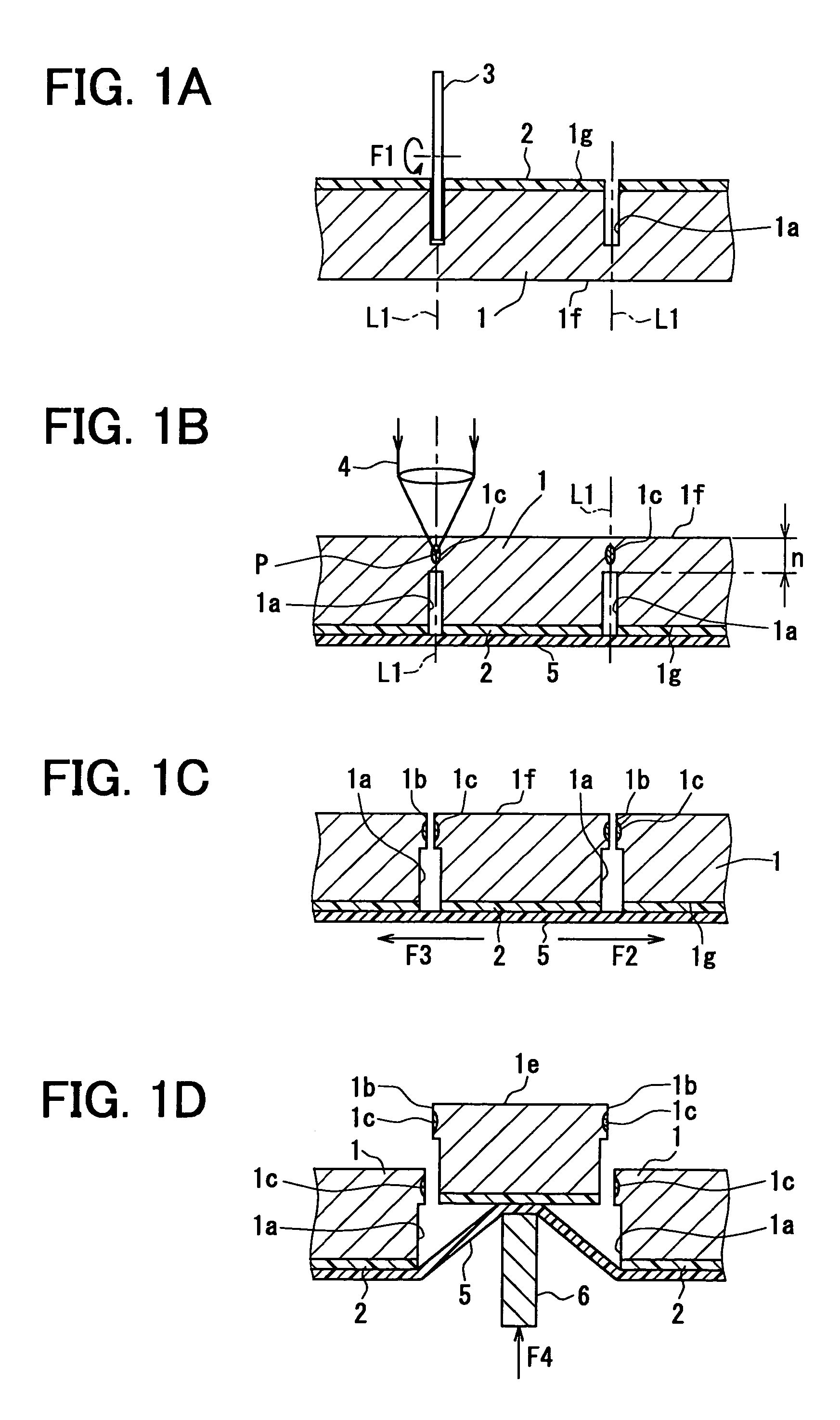
[0022]FIGS. 1A to 1D show cross-sectional views of a separation process of a semiconductor substrate in a first embodiment of the present invention.

[0023]The process in the first embodiment is further detailed in the following steps. That is, in the step shown in FIG. 1A, the semiconductor substrate 1 having a DAF 2 adhered on a reverse side 1g is diced along a separation line L1 by a diamond blade 3 that rotates in a high-speed rotation in a direction indicated by a circular arrow F1. The dicing blade reaches to a depth in the substrate 1. Each of the separation lines L1 is formed in this manner. A cut 1a is formed in the semiconductor substrate 1 along the separation line L1.

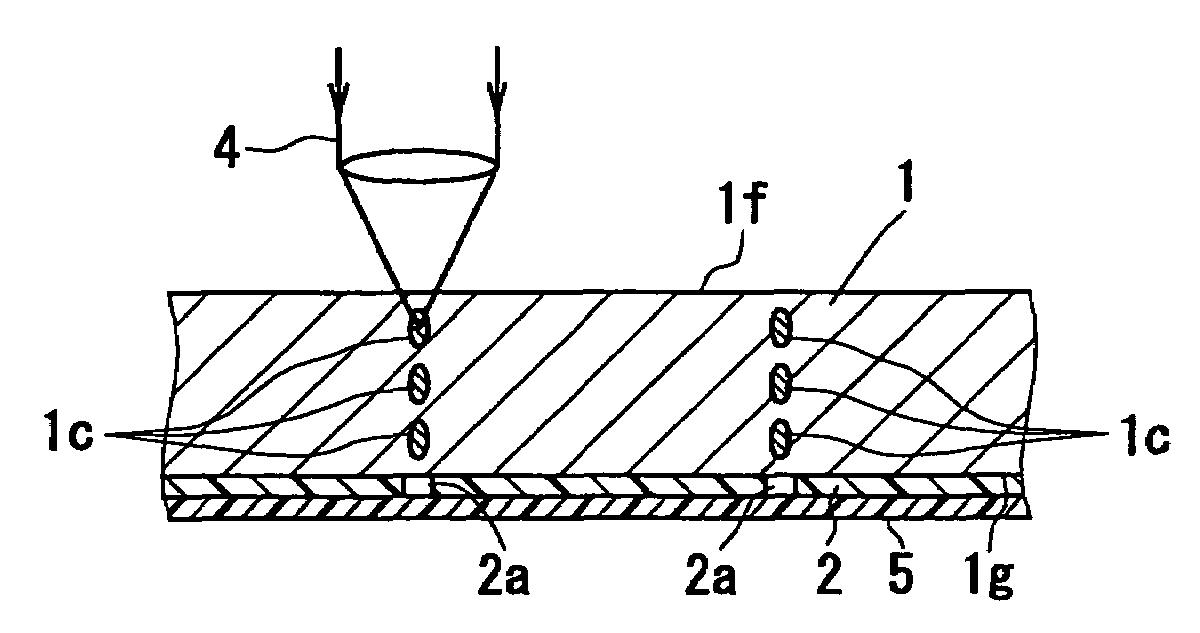
[0024]Then, in the step shown in FIG. 1B, a dicing film is adhered on a reverse side (implementation side) of the DAF 2. The semiconductor substrate 1 is flipped to receive a laser beam 4 irradiated from a surface 1f side to have a focusing point P on an extension of the cut 1a in the substrate. The focusing p...

second embodiment

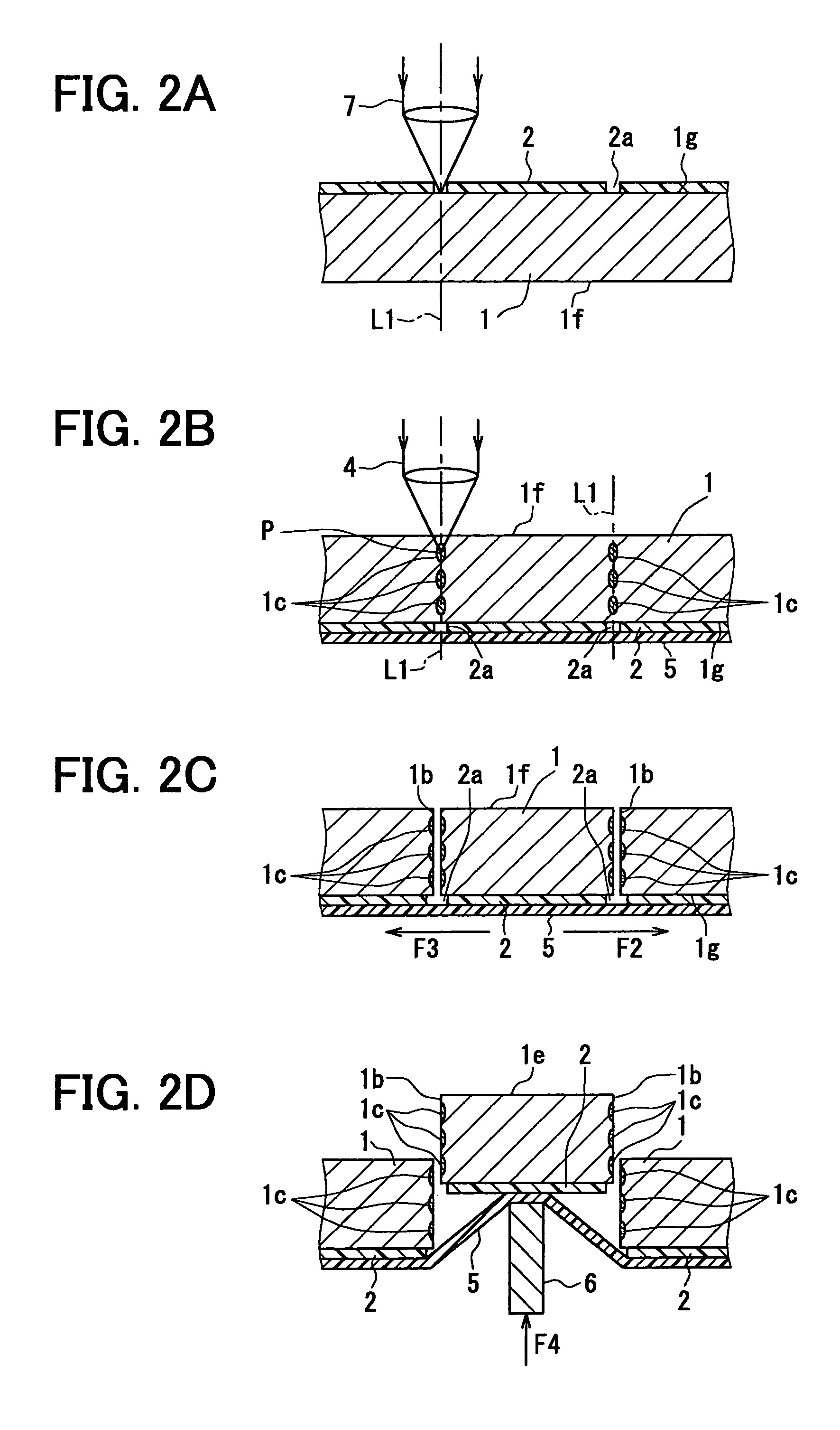
[0032]FIG. 2A to 2D show cross-sectional views of a separation process of the semiconductor substrate in a second embodiment. The separation method described in the second embodiment does not use the diamond blade for separation. Like parts have like numbers as used in the first embodiment, and descriptions of like parts are omitted.

[0033]In the process shown in FIG. 2A, the DAF 2 is meltingly separated by a laser beam 7 having the focusing point put on the DAF 2 along the separation line L1 irradiated from the reverse side 1g. The intensity of the laser beam 7 is strong enough to melt and separated the DAF 2.

[0034]In the process shown in FIG. 2B, the dicing film 5 is adhered on the reverse side (implementation side) of the DAF 2. Then, the semiconductor substrate 1 is flipped to have the laser beam 4 from an upper side of the substrate 1. The focusing point P of the laser beam 4 is aimed at a bottom of the substrate to form the modified area 1c along the separation line L1 in the f...

third embodiment

[0039]FIGS. 3A to 3D show cross-sectional views of a separation process of the semiconductor substrate in a third embodiment. In this embodiment, the DAF 2 is separated by a formation of the modified area with the laser beam from the surface of the semiconductor substrate. Like parts have like numbers as used in the second embodiment, and descriptions of like parts are omitted.

[0040]In the process shown in FIG. 3A, the dicing film 5 is adhered on the DAF 2. Then, the laser beam 7 is used to meltingly separate the semiconductor substrate 1. The laser beam 7 is irradiated from the surface 1f along the separation line L1 with the focusing point P aligned on the DAF 2. Each of the separation lines L1 on the DAF 2 is separated in this manner.

[0041]In the process shown in FIG. 3B to 3D, the semiconductor chip 1e is picked up by separating the semiconductor substrate 1 along the separation line L1 in the same process as described in the second embodiment shown in FIGS. 2B to 2D.

[0042]The s...


PUM

PropertyMeasurementUnit
wavelengthaaaaaaaaaa
semiconductoraaaaaaaaaa
areaaaaaaaaaaa

Abstract

A method of separating a semiconductor substrate having an implementation member attached thereon includes a dividing process for at least the implementation member on the semiconductor substrate along a separation line, a placing process for film member on a same side as the implementation member, a forming process area by irradiating a laser beam from at least one of a first side of the semiconductor substrate having the implementation member and a second side that is an opposite side of the first side of the semiconductor substrate along the separation line with a focusing point of the laser beam aligned with a substance in the semiconductor substrate and severing / removing at least one semiconductor chip at the separation line from the semiconductor substrate.

Description

CROSS REFERENCE TO RELATED APPLICATION[0001]This application is based on and claims the benefit of priority of Japanese Patent Application No. 2004-237300 filed on Aug. 17, 2004, the disclosure of which is incorporated herein by reference.FIELD OF THE INVENTION[0002]The present invention generally relates to a separation method of a semiconductor substrate.BACKGROUND OF THE INVENTION[0003]In recent years, semiconductor substrates are conventionally separated from a silicon wafer or the like by using a diamond blade. The separation method of the substrate suffers from problems such as a loss of cutting portion, that is, a blade width lost in the course of cutting, and a chipping of the substrate that deteriorates a yield rate of the substrate.[0004]A method to cope with the above-described problems is disclosed in Japanese Patent Document JP-3408805 as shown in FIGS. 4A to 4C. In this method, a laser light is used to form a modified area in the semiconductor substrate by multiphoton ...

Claims


Application Information

Patent Timeline
Patent Type & Authority Patents(United States)
IPC IPC(8): H01L21/00
CPCB23K26/0057B23K26/4075B28D5/0011H01L21/67092H01L21/6836H01L21/78H01L2221/68336B23K26/40B23K26/53B23K2103/50
Inventor TAMURA, MUNEOSOUKI, YASUO
Owner DENSO CORP
Why Eureka
Try Eureka