Emulation processor interconnection architecture

a technology of interconnection and processor, applied in the direction of cad circuit design, program control, instruments, etc., can solve the problems of reducing operating speed, increasing the number of emulation processors required to efficiently verify the design, and consuming to fabricate the design into silicon, so as to reduce the amount of area, interconnection and power dedicated, and improve the efficiency of the design verification system.

Active Publication Date: 2009-06-30
CADENCE DESIGN SYST INC
View PDF1 Cites 4 Cited by
  • Summary
  • Abstract
  • Description
  • Claims
  • Application Information

AI Technical Summary

Benefits of technology

[0016]The presently described embodiments describe a method and system for interconnecting a large number of emulation processors that dramatically reduces the amount of chip required by the interconnect structures and that significantly reduces power consumed by the integrated circuit. Assuming an emulation system with 2,048 processors, a savings of roughly eight times the area and an equivalent savings in power can be realized by implementation of the arrangement disclosed.
[0018]The various embodiments described herein reduce the width of the multiplexers while retaining the same number of multiplexers as there are processors. Each multiplexer inputs just one NBO from each cluster. Further, the multiplexers dedicated to processors in a common cluster jointly input each NBO once to that cluster, thus reducing any overlap and redundant selection within a single cluster of processors.
[0022]As will be appreciated by those skilled in the art, reducing each of 2,048 multiplexers from a 2,048 wide multiplexer to a 256 wide multiplexer significantly reduces the amount of area, interconnect, and power dedicated to interconnecting each of the processors. These savings equate to increased operating speeds, thus contributing to the efficiency of the design verification system.

Problems solved by technology

(DUV) Because it is very expensive and time consuming to fabricate a design into silicon, it is desirable to use an emulator to debug the logic to remove functional errors prior to fabrication.
As logic designs grow increasingly more complex, the number of emulation processors required to efficiently verify those designs has increased dramatically.
Implementing multiplexers and interconnect on different layers, though, reduces operating speeds and increases power usage of the entire system, rendering it a non-desirable solution.

Method used


Image

  • Emulation processor interconnection architecture
  • Emulation processor interconnection architecture
  • Emulation processor interconnection architecture

Examples


Embodiment Construction

[0029]With reference to the figures, the presently disclosed hardware design verification system and methods for the same will be discussed herein.

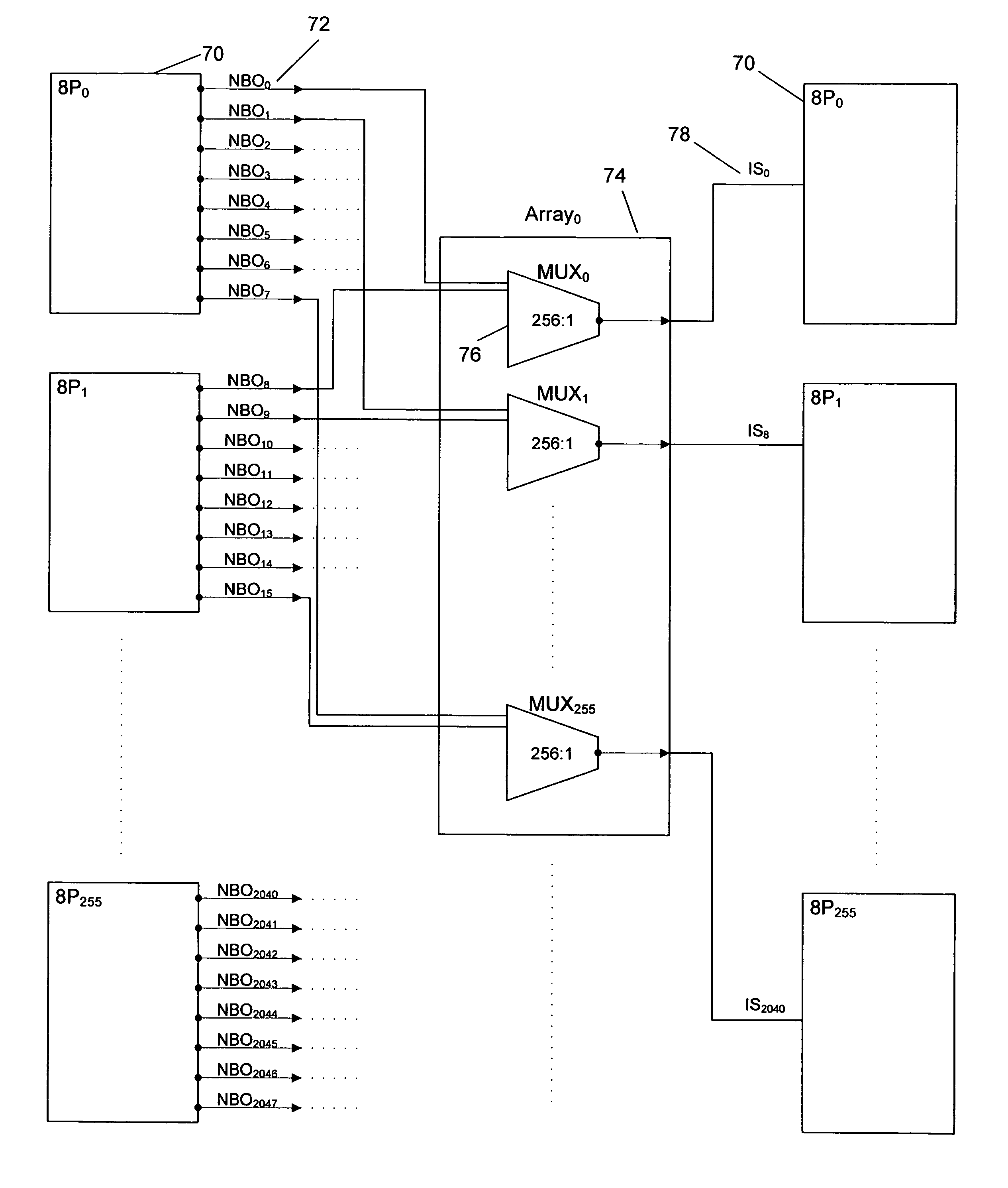
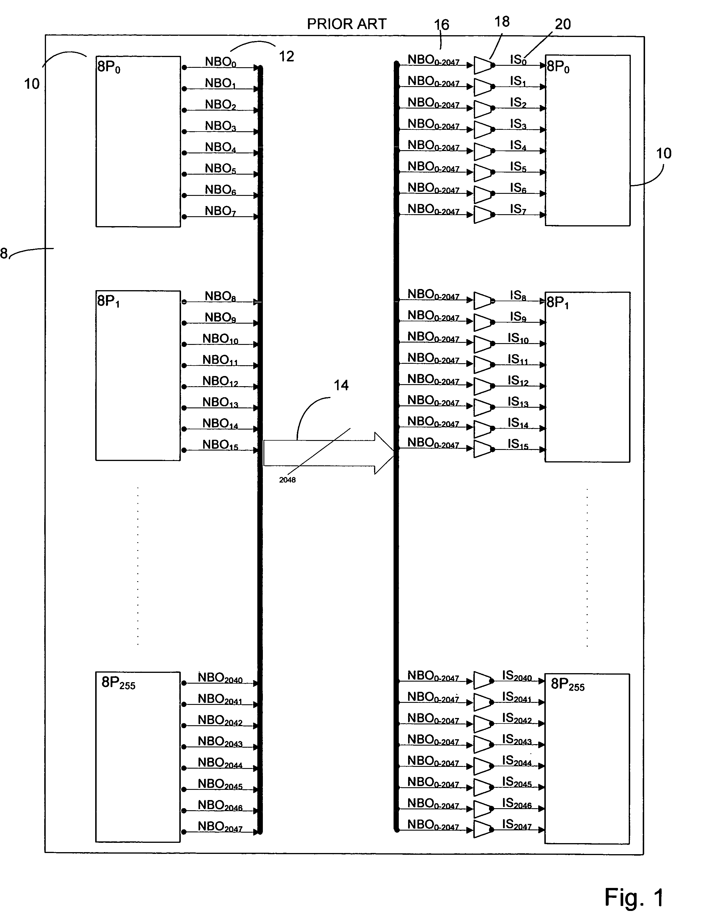
[0030]FIG. 1 depicts a prior art hardware design verification system 8 implementing 2,048 emulation processors according to the current state of the art. A number of emulation clusters 10 make up the system. The emulation clusters 10 are interconnected by signal busses 14, 16 and multiplexers 18. Each cluster outputs a number of node bit outs (NBO) 12 for a total of 2,048 NBOs. Each of the 2,048 NBOs meet to form a first NBO bus 14. The first NBO bus 14 carrying all 2,048 bits is then passed into the multiplexers 18 on signal busses 16. The multiplexers 18 select one of the 2,048 signals and output IS signal 20, which is passed back into each emulation cluster 10. Thus, each bus 16 carries all 2,048 NBOs as inputs to each of the multiplexers 18, which select a signal for input to the emulation clusters 10.

[0031]It should be noted with ref...


PUM


Abstract

The present system and methods are directed to the interconnection of clusters of emulation processors comprising emulation processors in a software-driven hardware design verification system. The processors each output one NBO output signal. The clusters are interconnected by partitioning a common NBO bus into a number of smaller NBO busses, each carrying unique NBO signals but together carrying every NBO. Each of the smaller NBO busses are passed into a series of multiplexers, each dedicated to a particular processor. The multiplexers select a signal for output back to the emulation clusters. The multiplexers that handle these smaller NBO busses are narrower than was previously required, thus reducing the amount of power, interconnect, and area required by the multiplexer array and dedicated interconnect.

Description

CROSS-REFERENCE TO RELATED APPLICATIONS[0001]This application claims priority to U.S. Provisional Application Ser. No. 60 / 648,976, which was filed on Jan. 31, 2005. Priority to this prior application is expressly claimed, and the disclosure is hereby incorporated by reference in its entirety.FIELD[0002]The present disclosure relates generally to design verification systems, and more specifically to the interconnection of a large number of discreet emulation processors in a software-driven hardware design verification system.BACKGROUND OF THE INVENTION[0003]Hardware based functional design verification systems, often referred to as emulators or simulation accelerators, are devices that allow functional verification of a user's logic design prior to fabrication of the design into an integrated circuit. (IC). The logic design at this stage is often referred to as the design under tests, (DUT), or design under verification. (DUV) Because it is very expensive and time consuming to fabric...

Claims


Application Information

Patent Timeline
Patent Type & Authority Patents(United States)
IPC IPC(8): G06F9/455G06F9/45
CPCG06F17/5022G06F2217/86G06F30/33G06F2117/08
Inventor BEAUSOLEIL, WILLIAM F.POPLACK, MITCHELL G.COMFORT, STEVEN TELMUFDI, BESHARA
Owner CADENCE DESIGN SYST INC
Why Eureka
Try Eureka