
JFET with built in back gate in either SOI or bulk silicon

a back gate and silicon technology, applied in the direction of semiconductor devices, electrical apparatus, transistors, etc., can solve the problems of reducing the overall total number of devices that can be formed on any wafer, consuming chip area, etc., and achieving the elimination of parasitic capacitance of the back gate contact, eliminating the parasitic capacitance of the junction, and consuming the effect of area

Inactive Publication Date: 2009-07-07
MIE FUJITSU SEMICON
View PDF9 Cites 5 Cited by
  • Summary
  • Abstract
  • Description
  • Claims
  • Application Information

AI Technical Summary

Benefits of technology

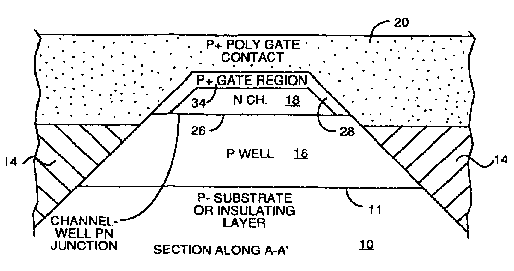
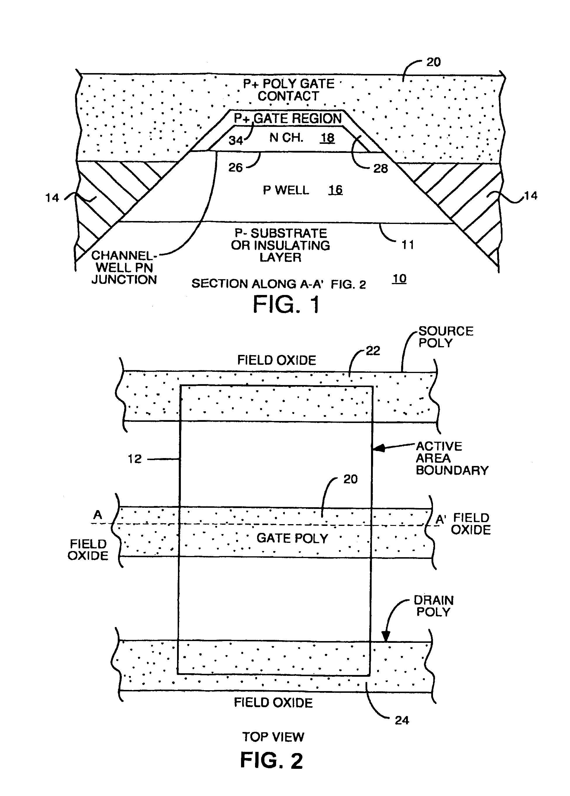
[0007]With a JFET structured as taught herein, the well will always have the same bias as the gate region because the gate region extends down the sidewalls of the channel region where the gate polysilicon crosses over the active area and dips down into the notch etched in the field oxide. This causes the channel-well PN junction to be shorted thereby causing the well to have the same bias as the gate. Thus, when the gate-channel PN junction is forward biased, so is the channel-well PN junction. In an enhancement-mode device, this means that the depletion regions around these two PN junctions decrease in size thereby opening up a conductive path through the channel. Generally, about twice as much current flows through this channel in a device according to the teachings of the invention as in a normal four terminal enhancement-mode JFET where the gate-channel junction is forward biased and the well is grounded. When the well is grounded, there is no effect on the channel-well PN junction and its depletion region extends into the channel region thereby depleting a portion of the channel region of minority carriers. This portion of the volume of the channel cannot conduct current between the source and drain. In a three terminal device as taught herein, when the gate-channel junction is forward biased, so is the channel-well junction. This means that the volume of the channel region which is normally consumed by the depletion region around the channel-well junction in a four terminal device is not consumed by depletion region in the three terminal device and is available for conduction. Therefore, approximately twice the source-drain current flows in the three terminal enhancement JFET when the gate is biased to a level sufficient to bring the device out of pinch-off, and the transconductance (the change in source to drain current divided by the change in gate voltage that caused said change in source to drain current) is doubled. In an alternative embodiment, the material under the semiconductor well can be an insulator. In these embodiments, one starts with an insulating substrate and forms a semiconductor region above it by means of epitaxial growth. This semiconductor region will be doped to form the well, and field oxide will be formed to define a portion of the well as an active area. Thereafter, processing to form a structure according to the teachings of the invention is as described elsewhere herein. By virtue of elimination of the well-substrate PN junction, the parasitic capacitance of that junction is eliminated. This makes the device faster.
[0008]The invention enables elimination of the area consumed by the back gate contact and all the design rule tolerances around it as well as parasitic capacitances associated with the back gate. By virtue of elimination of the back gate contact parasitic capacitances, a structure according to the teachings of the invention has a faster switching speed than four terminal JFETs. This is because the structure is such as to eliminate the parasitic junction capacitance associated with the P+ back gate contact interface with the P− well. Further, the structure of the preferred embodiment built on an insulating substrate also eliminates the parasitic junction capacitance of the junction between the P− well and the underlying N-doped bulk substrate thereby speeding up the maximum switching speed of the device.

Problems solved by technology

This separate contact for the well consumes chip area and reduces the overall total number of devices that can be formed on any wafer.

Method used


Image

  • JFET with built in back gate in either SOI or bulk silicon
  • JFET with built in back gate in either SOI or bulk silicon
  • JFET with built in back gate in either SOI or bulk silicon

Examples


case 2

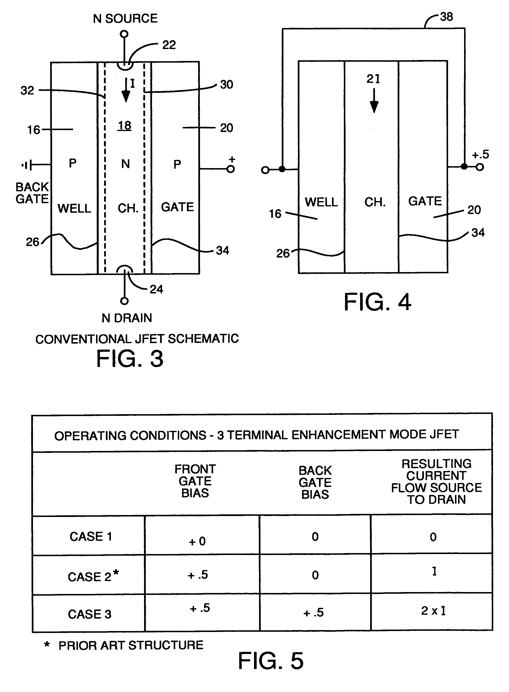
[0033]Case 2 represents the prior art case shown in FIG. 3 where +0.5 volts is applied to the front gate and the back gate is grounded. In this case, source-to-drain current flow is i.

case 3

[0034]Case 3 is the case according to the teachings of the invention where when +0.5 volts is applied to the front gate, the same bias of +0.5 is automatically applied to the back gate. This case is represented by FIG. 4. This case results in a source-to-drain current flow of 2 times i. The reason the current flow is 2 i in Case 3 is because both the front gate and the back gate are forward biased. This causes the depletion region to pull back or disappear around both of junctions 26 and 34. This effectively doubles the volume in the channel through which current can flow and reduces the resistance proportionately. This increases the current flow to twice the level of the prior art when the back gate is grounded. Of course a current flow of 2 i can be achieved in the prior art structure by using the surface contact of the back gate to forward bias the back gate junction.

The Preferred Epi on Insulator Embodiment Structure and Process

[0035]Appendix A is a table giving the process step...


PUM


Abstract

A Junction Field-Effect transistor with no surface contact for the back gate and twice as much transconductance in the channel and with a higher switching speed is achieved by intentionally shorting the channel-well PN junction with the gate region. This is achieved by intentionally etching away field oxide outside the active area at least in the gate region so as to expose the sidewalls of the active area down to the channel-well PN junction or a buried gate which is in electrical contact with the well. Polysilicon is then deposited in the trench and doped heavily and an anneal step is used to drive impurities into the top and sidewalls of the channel region thereby creating a “wrap-around” gate region which reaches down the sidewalls of the channel region to the channel-well PN junction. This causes the bias applied to the gate terminal to also be applied to the well thereby modulating the channel transconductance with the depletion regions around both the gate-channel PN junction and the channel-well PN junction.

Description

FIELD OF USE AND BACKGROUND OF THE INVENTION[0001]Junction Field-Effect Transistors (JFETs) are made in active areas in semiconductor substrates where the active area is surrounded by field oxide. In the active area, a conductive area called a well is formed and that well forms a PN junction with the bulk substrate. That PN junction is called the back gate, and it is conventional to form a surface contact to the well so that bias can be applied to the well region for various purposes. This separate contact for the well consumes chip area and reduces the overall total number of devices that can be formed on any wafer.[0002]In the well, a conductive channel region is formed, and in that channel region, conductive source, drain and gate regions are formed. These source, drain and gate regions form PN junctions with the channel region. In a new class of processes and structures which are the subject of patent applications previously filed by the assignee of the present invention, these ...

Claims


Application Information

Patent Timeline
Patent Type & Authority Patents(United States)
IPC IPC(8): H01L31/112
CPCH01L29/1066H01L29/808H01L29/66901H01L29/42316H01L21/18H01L29/10H01L29/423
Inventor VORA, MADHUKAR B.
Owner MIE FUJITSU SEMICON
Learn More