Semiconductor device and method of manufacturing the same

a technology of semiconductor devices and semiconductors, applied in the direction of semiconductor devices, electrical devices, transistors, etc., can solve the problems of increasing drain contact resistance, and achieve the effect of reducing contact resistance and reducing level differences

Inactive Publication Date: 2009-07-07
KK TOSHIBA
View PDF3 Cites 13 Cited by
  • Summary
  • Abstract
  • Description
  • Claims
  • Application Information

AI Technical Summary

Benefits of technology

[0011]Therefore, an object of the present invention is to provide a semiconductor device which can reduce the difference in level between the insulating film in the element isolation region of the drain contact formation region and the element formation region thereby to reduce a contact resistance and prevent the gate insulating film from being adversely affected, and a method of manufacturing the same.

Problems solved by technology

When an employed manufacturing process includes a step of forming an STI structure for isolation of elements after previous formation of a part of the gate structure, the following drawback is found: in the above-described manufacturing process, immediately after formation of the gate electrode, there is a difference in level between the upper surface of the silicon substrate or an active area (an element isolation region) and an upper surface of the STI which is an element isolation region, in a part where a layer serving as a gate electrode has been removed by the etching process.
This results in limitations in a contact area in the case where the drain contact of the active area is formed, thereby increasing a drain contact resistance.

Method used


Image

  • Semiconductor device and method of manufacturing the same
  • Semiconductor device and method of manufacturing the same
  • Semiconductor device and method of manufacturing the same

Examples


Embodiment Construction

[0019]One embodiment of the present invention will be described with reference to the accompanying drawings. The invention is applied to a NOR flash memory in the embodiment.

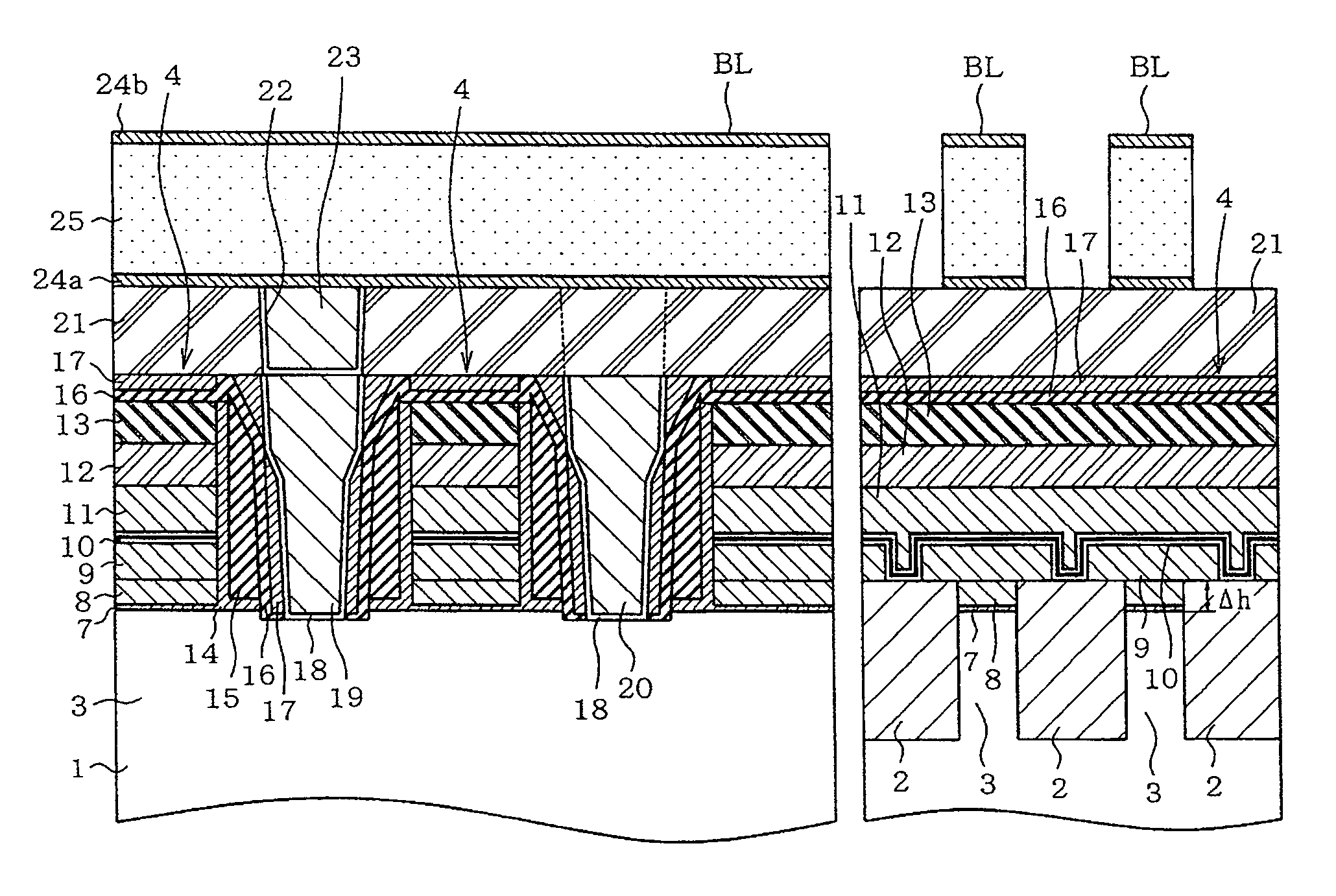
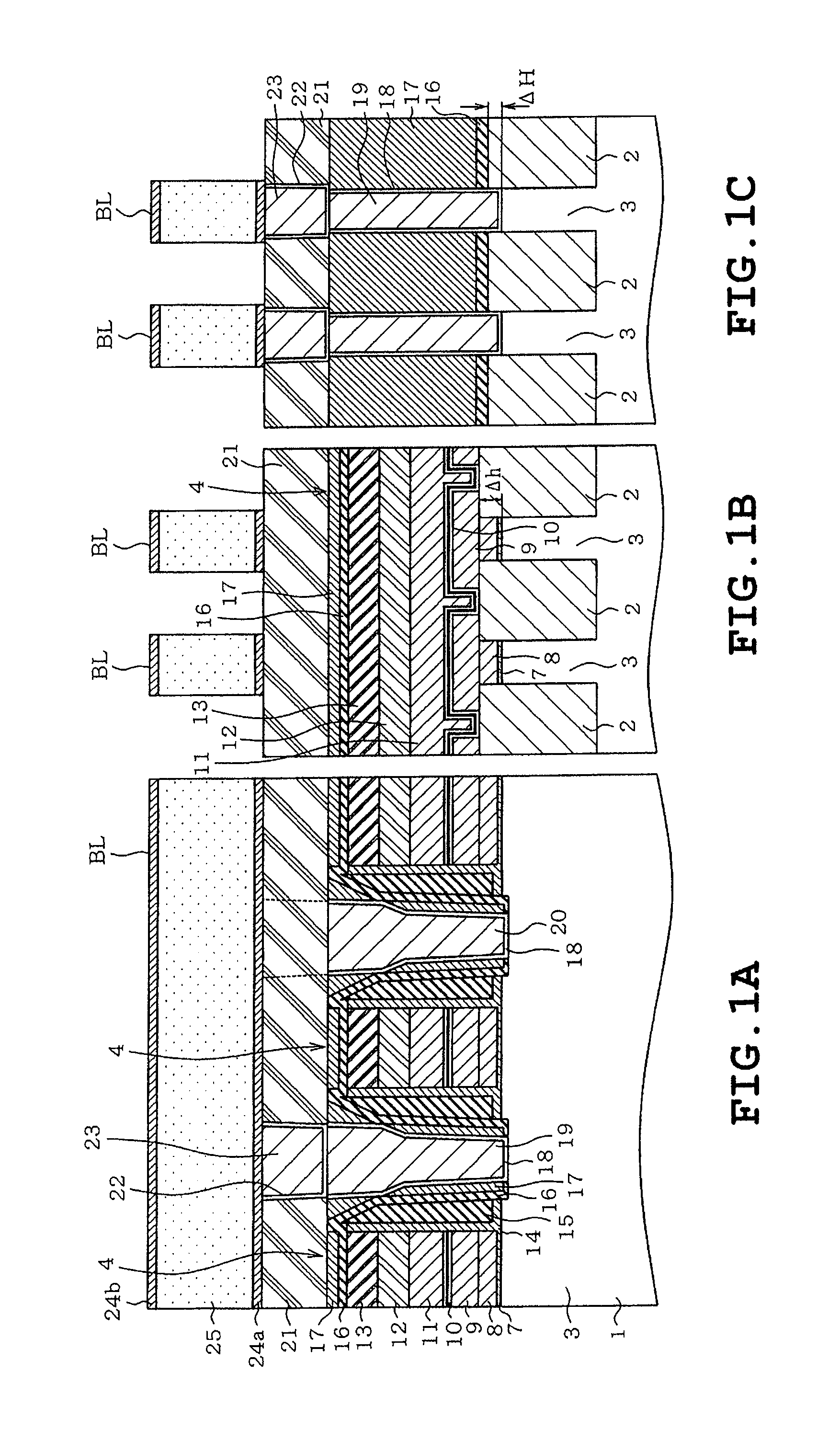
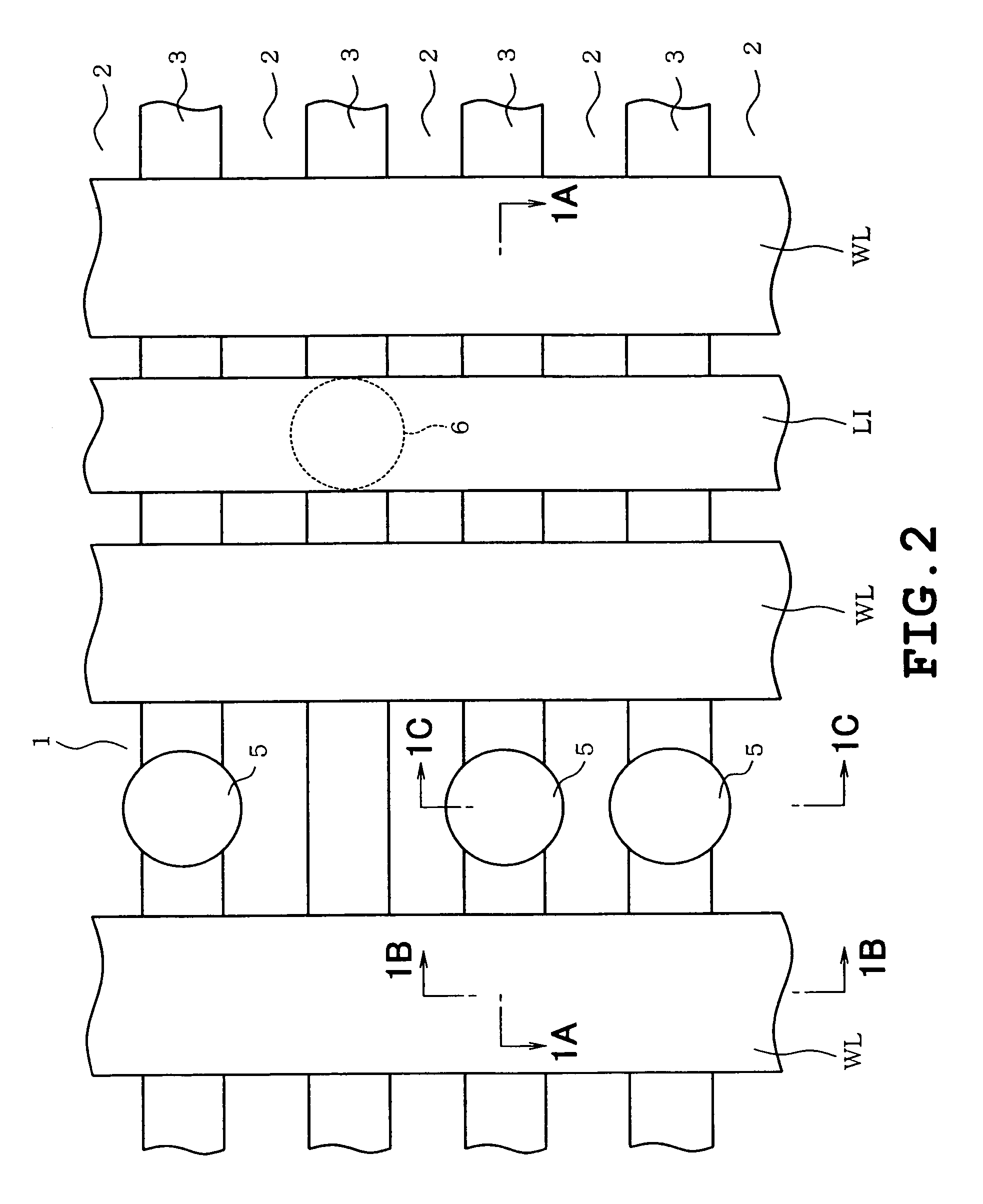
[0020]FIGS. 1A to 1C schematically show memory cell transistors in a memory cell region of the NOR flash memory. FIG. 2 shows positions where the views of FIGS. 1A to 1C are taken. Referring to FIG. 2, a silicon substrate 1 serving as a semiconductor substrate is formed with a shallow trench isolation (STI) 2 serving as an element isolation insulating film, whereby active areas 3 are defined as element formation regions.

[0021]Word lines WL are formed at predetermined intervals so as to intersect the active areas 3. Of gate electrodes 4 formed in the respective memory cell transistors, each word line WL corresponds to a control gate electrode to be formed between adjacent memory cell transistors with the STI 2 being interposed therebetween. Each active area 3 exposed between adjacent word lines WL includes a drai...


PUM


Abstract

A semiconductor device includes an element isolation insulating film adjacent to an active area, a gate insulating film formed on a semiconductor substrate in the active area, paired gate electrodes located on the gate insulating film, a contact plug located on the active area between the gate electrodes, a pair of first upper lines located on the gate electrodes, a second upper line located on the gate electrodes, and a stopper film above upper surfaces of the gate electrodes and side surfaces of the gate electrodes. The element isolation insulating film has a first height of an upper surface thereof with reference to an upper surface of the semiconductor substrate and a second height of another upper surface thereof with reference to another upper surface of the semiconductor substrate. The first height is smaller than the second height.

Description

CROSS-REFERENCE TO RELATED APPLICATIONS[0001]This application is based upon and claims the benefit of priority from the prior Japanese Patent Application No. 2005-119690, filed on Apr. 18, 2005, the entire contents of which are incorporated herein by reference.BACKGROUND OF THE INVENTION[0002]1. Field of the Invention[0003]The present invention relates to a semiconductor device having a structure that memory cell transistors are isolated by an element isolation insulating film thereby to be formed and a method of manufacturing the same.[0004]2. Description of the Related Art[0005]For example, a NOR flash memory is one of memories employing a shallow trench isolation (STI) structure which is one of structures that memory cell transistors are isolated by an element isolation insulating film thereby to be formed. The NOR flash memory employs an arrangement that a contact hole is formed in a drain of each of a number of memory cell transistors so that an electrode is connected to the co...

Claims


Application Information

Patent Timeline
Patent Type & Authority Patents(United States)
IPC IPC(8): H01L29/76
CPCH01L21/76897H01L27/1052H01L27/11521H01L27/115H01L21/28273H01L29/40114H10B99/00H10B69/00H10B41/30
Inventor YONEHAMA, KEISUKEMORI, SEIICHISAKAGAMI, EIJISONODA, MASAHISA
Owner KK TOSHIBA
Why Eureka
Try Eureka