Electronic part manufacturing method and electronic part manufactured by the method

a manufacturing method and electronic technology, applied in the direction of transfer patterning, transportation and packaging, instruments, etc., can solve the problems of high manufacturing time, difficult to laminate each layer at a correct position, and defects in the upper pattern laminated on the lower pattern, so as to reduce the number of superpose printing steps, eliminate defects, and improve production efficiency

Inactive Publication Date: 2012-03-01
DAINIPPON INK & CHEM INC
View PDF0 Cites 5 Cited by
  • Summary
  • Abstract
  • Description
  • Claims
  • Application Information

AI Technical Summary

Benefits of technology

[0020]According to the present invention, it is possible to decrease the number of superpose-printing steps for functional material ink pattern layers, realize high-precision alignment between the functional material ink pattern layers, and form a laminated structure with forming substantially no difference in level, thereby eliminating defects in each of the functional material pattern layers. According to the present invention, it is possible to provide an electronic part with higher productivity and higher performance.

Problems solved by technology

However, the method for manufacturing an electronic part has the need to form patterned layers having respective functions on the blanket one-by-one, and laminate the layers on the printing object, and thus has the important problems (1) that much time is required for manufacture because of a large number of superpose-printing steps, (2) that it is difficult to laminate each of the layers at a correct position, and (3) that defects occur in an upper pattern laminated on a lower pattern due to a difference in level of the lower pattern.

Method used


Image

  • Electronic part manufacturing method and electronic part manufactured by the method
  • Electronic part manufacturing method and electronic part manufactured by the method
  • Electronic part manufacturing method and electronic part manufactured by the method

Examples


example 1

Formation of BGSC Organic Transistor Element

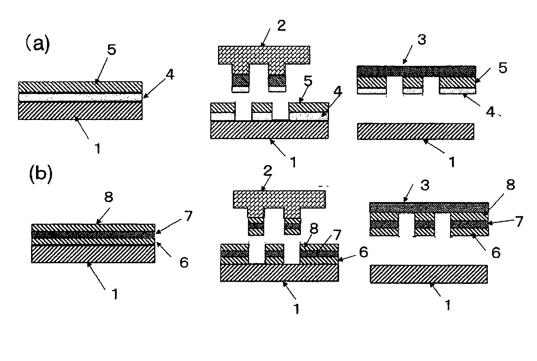
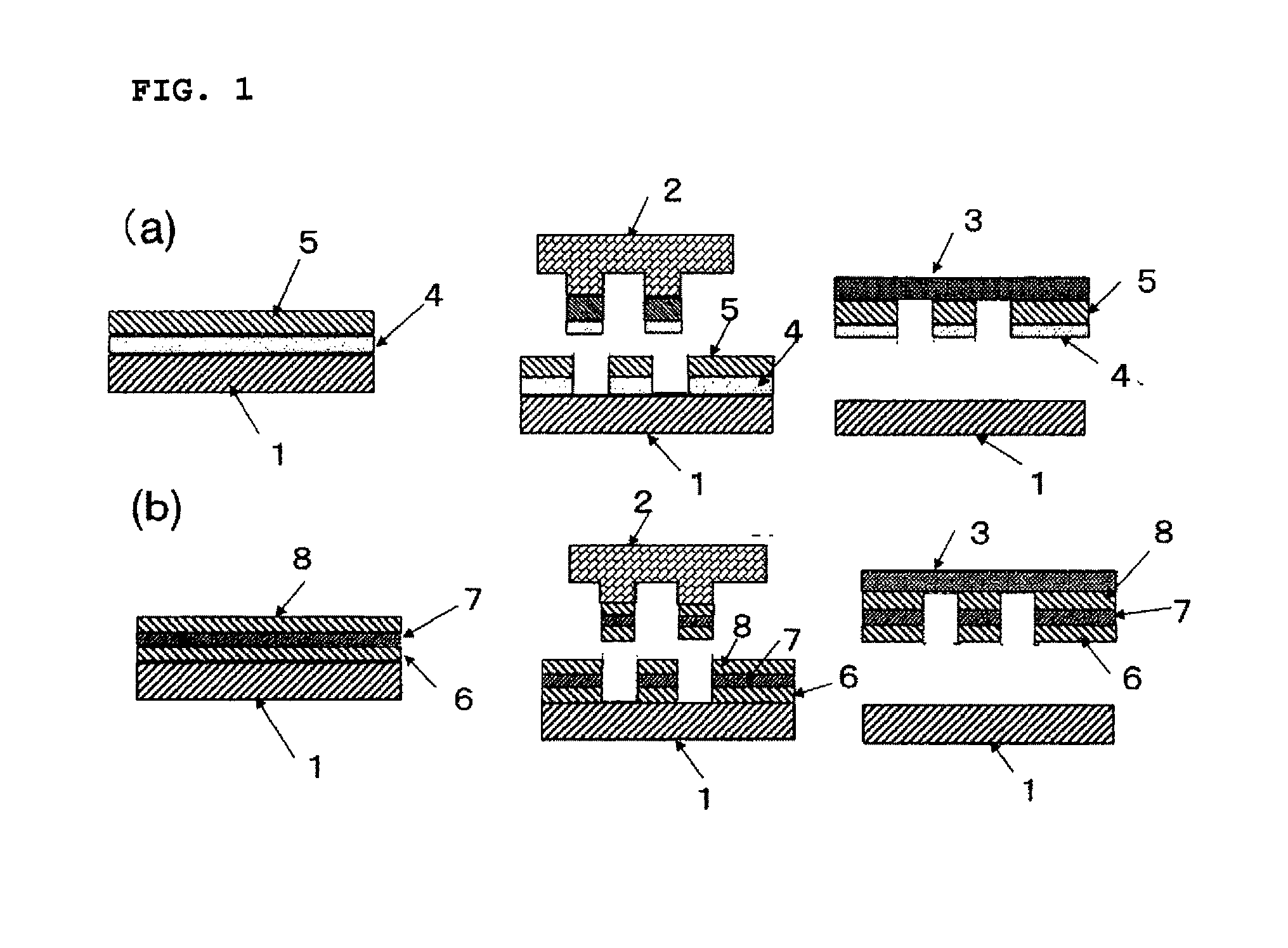
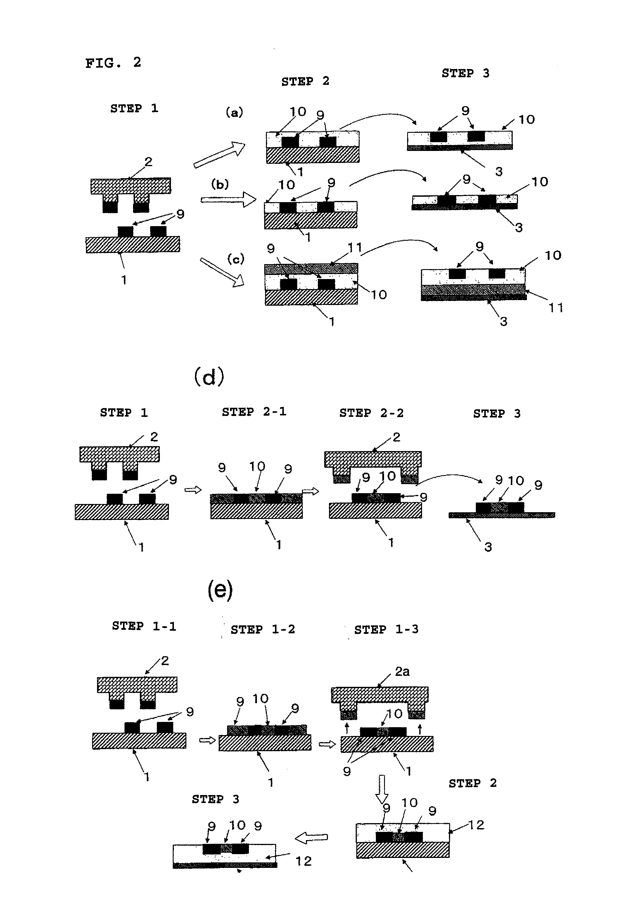
[0060]As shown in FIG. 3, a source / drain electrode pattern 9s / 9d was formed on a transfer plate 1 (3-1 of FIG. 3). The electrode pattern was formed using a conductive ink containing a fluorine-based surfactant. Then, a semiconductor ink containing P3HT as a main component was uniformly applied to the transfer plate 1, on which the pattern had been formed, using a capillary coater so that the thickness at a maximum after evaporation of the solvent was smaller than the thickness of the electrode, thereby forming an ink film layer 13 of P3HT (3-2 of FIG. 3). In this case, coating of the organic semiconductor ink on the electrode pattern was not observed.

[0061]Then, the organic semiconductor ink, excluding the organic semiconductor ink pattern remaining between the source and drain, was removed from the transfer plate 1 to leave the source / drain electrode pattern by the relief offset method using the same pattern as the relief plate for formin...

example 2

Method for Manufacturing BGBC-Type Organic Transistor Element

[0063]A method for manufacturing a BGBC-type MIS organic transistor element is shown in FIG. 4.

(1) Formation of Gate Electrode

[0064]A relief offset printing conductive ink containing silver nano particles dispersed therein was uniformly applied by a capillary coater to the entire surface of a transfer plate 1 having a smooth releasing surface composed of a silicone resin. Then, a glass relief plate (not shown) was pressed on the ink surface to remove an excessive ink, forming a gate electrode pattern 9q on the transfer plate 1. Then, an insulating ink containing an epoxy resin and a polyvinyl phenol resin as main components was uniformly applied to the gate pattern 9g on the transfer plate 1 by using a capillary coater, forming an insulating ink film layer 10i. After being allowed to stand for about 1 minute, the insulating film ink, and the gate electrode pattern in a semidried state were reversely transferred to a plasti...

example 3

BGBC+Protective Film (with Via)+Pixel Electrode

[0067]As shown in FIG. 5a, a conductive pattern 14 serving as via was formed on a transfer plate having a smooth surface composed of a silicone resin by the relief offset method using a nano silver ink containing a liquid-repellent component including a fluorine-based surfactant. A coating film of a projective film forming ink containing an epoxy resin as a main component was uniformly applied to the nano-silver ink pattern previously formed so that the thickness was smaller than that of at least the conductive pattern, thereby forming a protective film ink layer 15. In this case, adhesion of the ink to the pattern was not observed. The protective film forming ink layer and the conductive pattern layer were simultaneously reversely transferred so that the conductive pattern 14 was in contact with the drain electrode 9d of the organic transistor formed in Example 1, followed by sintering at 140° C. for about 30 minutes.

[0068]Then, a patt...


PUM

PropertyMeasurementUnit
viscosityaaaaaaaaaa
electromagnetic characteristicaaaaaaaaaa
physical propertiesaaaaaaaaaa

Abstract

The present invention provides a new method for manufacturing an electronic part, which is capable of reducing the number of steps of superpose-printing, achieving positional accuracy (alignment accuracy) of precise superposed patterns, and layering with substantially no difference in level, thereby improving productivity and dimensional accuracy and eliminating defects. The method for manufacturing an electronic part includes the steps of forming a composite ink pattern layer on a releasing surface of a transfer plate using a relief offset method, and then simultaneously reversely transferring the composite ink pattern layer to a printing object. Various organic transistor elements are formed by combining a conductive ink, an insulating ink, and an ink containing a semiconductor.

Description

TECHNICAL FIELD[0001]The present invention relates to a method for manufacturing an electronic part by a relief offset method and an electronic part manufactured by the method.BACKGROUND ART[0002]Various methods described below have been investigated as methods for manufacturing electronic parts by printing. For example, Patent Literature 1 discloses a method for forming a thin-film transistor circuit, in which a resist pattern is formed using a cylinder offset printing machine and dimensional error is suppressed by controlling a transfer rate and a reverse transfer rate. Patent Literature 2 discloses a method for producing a circuit board, the method including forming a conductor layer on a core insulating layer by a printing method, forming an insulating layer having a hole on the conductor layer by a printing method, and further filling the hole with an electromagnetic characteristic material by a printing method.[0003]Patent Literature 3 discloses a method for producing a printe...

Claims


Application Information

Patent Timeline
Patent Type & Authority Applications(United States)
IPC IPC(8): B32B37/26B32B3/14
CPCH01L51/0013H01L51/0016H01L51/003Y10T428/24802H05K3/207H05K2203/0108H05K2203/0528H05K3/046Y10T156/1052H10K71/221H10K71/18H10K71/80H05K1/0296H05K3/101
Inventor KOTAKE, MASAYOSHI
Owner DAINIPPON INK & CHEM INC
Why Eureka
Try Eureka