

Processing method of stacked-layer film and manufacturing method of semiconductor device
a technology of stacked-layer film and processing method, which is applied in the direction of semiconductor devices, basic electric elements, electrical equipment, etc., can solve the problems of deterioration of electrical characteristics of transistors, affecting the yield of semiconductor devices, and easy occurrence of shape defects by slight difference in level, so as to reduce the thickness of each layer, reduce the effect of shape defects and easy occurrence of defects
- Summary
- Abstract
- Description
- Claims
- Application Information
AI Technical Summary
Benefits of technology
Problems solved by technology
Method used
Image

Examples
embodiment 1
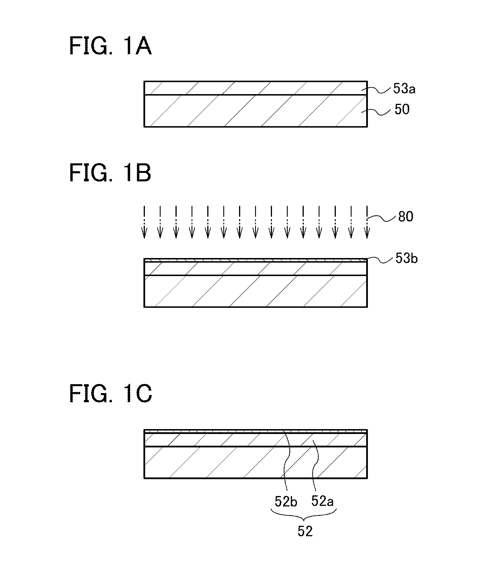
[0074]In this embodiment, a stacked-layer film according to one embodiment of the present invention will be described.
[0075]FIGS. 1A to 1C are cross-sectional views illustrating a method for forming the stacked-layer film according to an embodiment of the present invention.
[0076]First, an oxide insulating film 53a is formed over a substrate 50 (see FIG. 1A).
[0077]The oxide insulating film 53a may be formed of a single layer or a stacked layer using an insulating film including one or more of aluminum oxide, magnesium oxide, silicon oxide, silicon oxynitride, germanium oxide, yttrium oxide, zirconium oxide, lanthanum oxide, neodymium oxide, hafnium oxide, and tantalum oxide.
[0078]Note that, in this specification, silicon oxynitride refers to a substance that contains more oxygen than nitrogen, and silicon nitride oxide refers to a substance that contains more nitrogen than oxygen.
[0079]The oxide insulating film 53a can be deposited by a sputtering method, a chemical vapor deposition ...
embodiment 2
[0104]In this embodiment, a transistor according to one embodiment of the present invention using the stacked-layer film described in Embodiment 1 will be described.
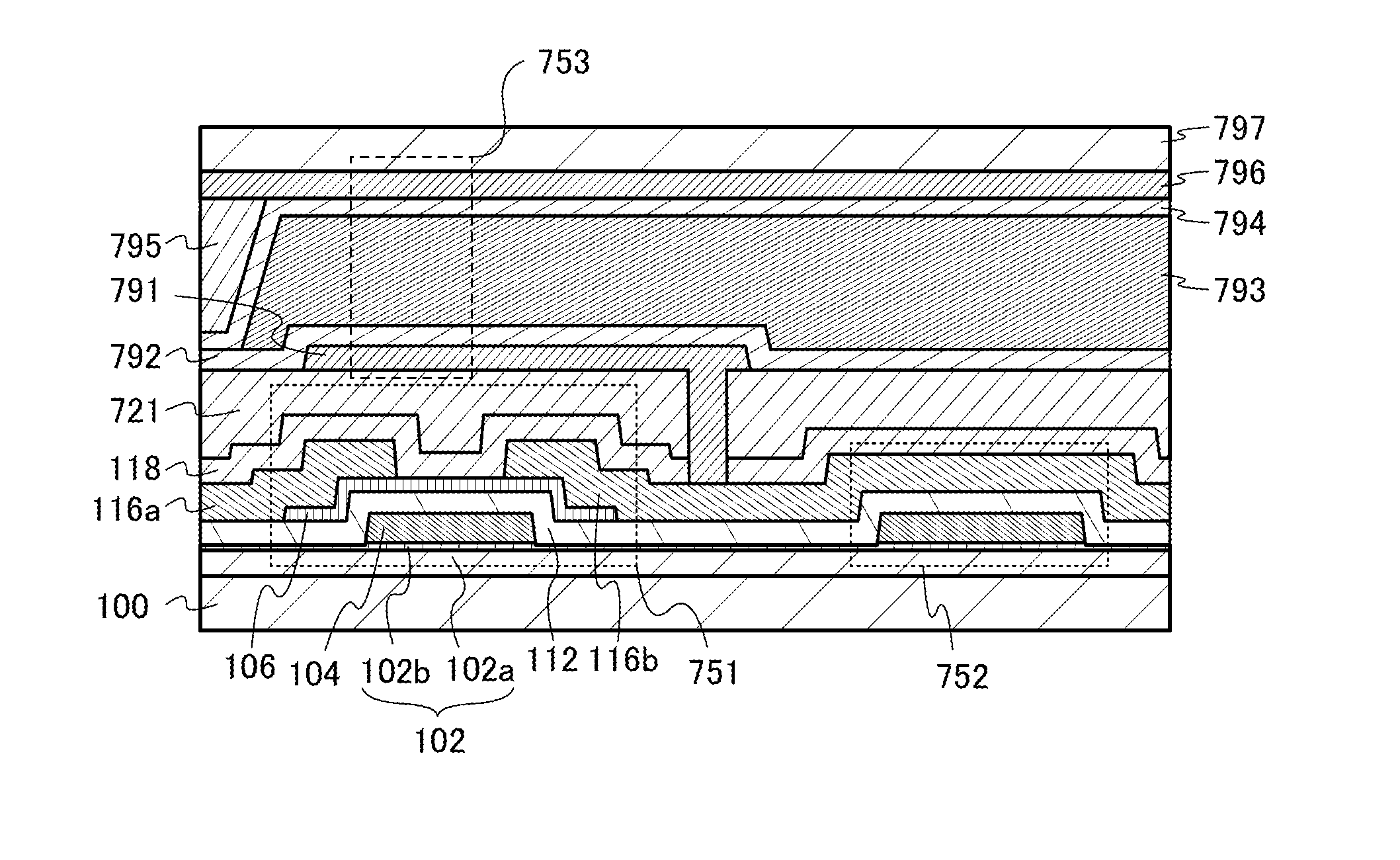
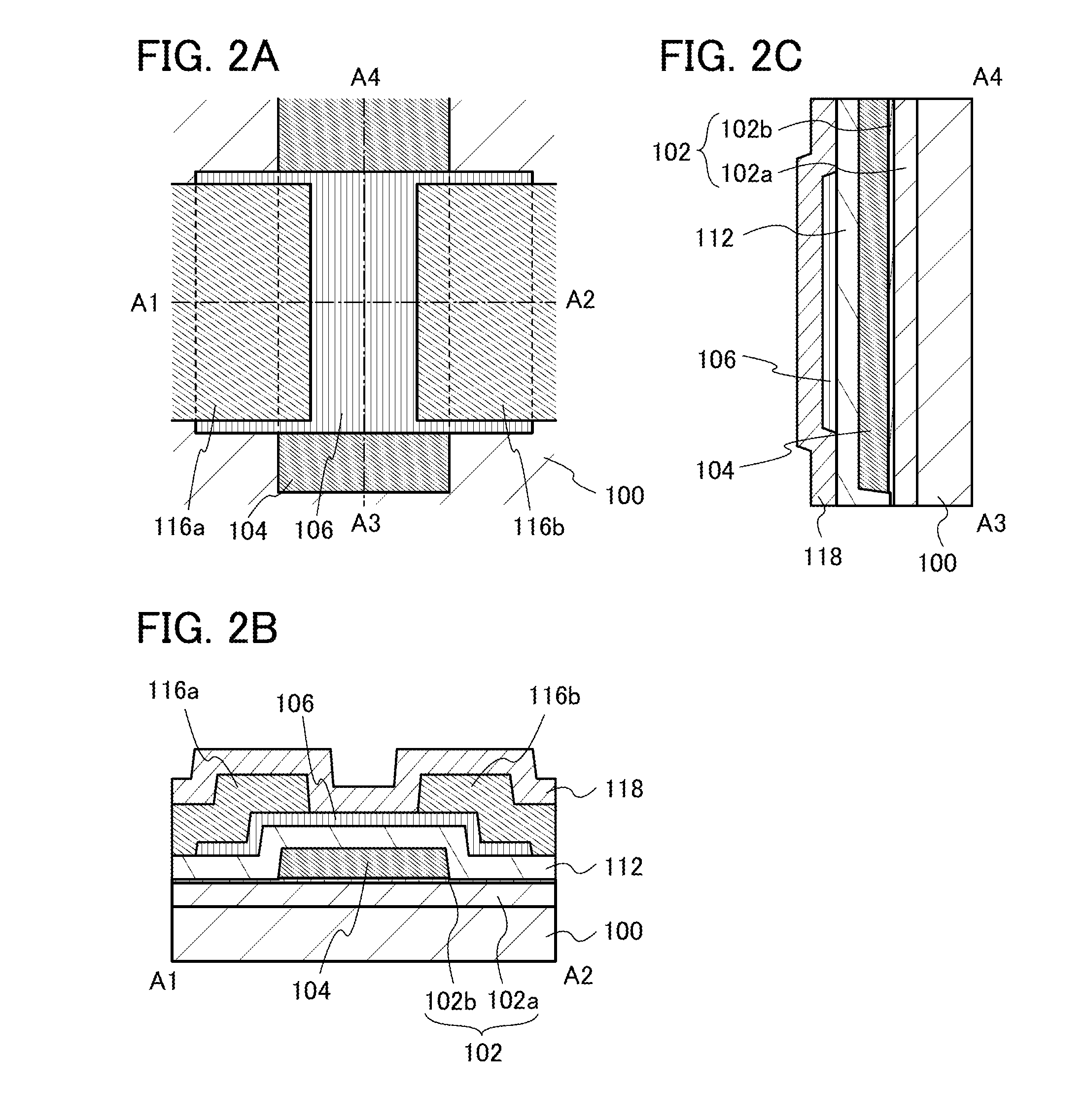
[0105]FIG. 2A is a top view of a transistor according to one embodiment of the present invention. FIG. 2B is a cross-sectional view along dashed-dotted line A1-A2 of FIG. 2A. FIG. 2C is a cross-sectional view taken along dashed-dotted line A3-A4 in FIG. 2A. Note that a gate insulating film 112 and the like are not illustrated in FIG. 2A for easy understanding.
[0106]FIG. 2B is a cross-sectional view of a transistor including a stacked-layer film 102 including an oxide insulating film 102a provided over a substrate 100 and a metal oxide film 102b provided over the oxide insulating film 102a, a gate electrode 104 provided over the stacked-layer film 102, a gate insulating film 112 provided over the gate electrode 104, an oxide semiconductor film 106 provided over the gate insulating film 112 and overlapping with the gate el...
embodiment 3
[0332]In this embodiment, a semiconductor device including a memory element to which any of the transistors described in the above embodiments is applied will be described.
[0333]In the transistor described in the above embodiment, not only stable electrical characteristics are given, but also the off-state current of the transistor can be significantly reduced. That is, the transistor has electrical characteristics in which leakage of charge through the transistor is unlikely to occur.
[0334]A semiconductor device which includes a transistor having such electric characteristics will be described below. The semiconductor device includes a memory element which is superior in function to a known memory element.
[0335]First, the semiconductor device will be specifically described with reference to FIGS. 17A to 17D. FIG. 17A is a circuit diagram showing a memory cell array of the semiconductor device. FIG. 17B is a circuit diagram of a memory cell. FIG. 17C illustrates an example of a cros...
PUM
| Property | Measurement | Unit |
|---|---|---|
| voltage | aaaaa | aaaaa |
| voltage | aaaaa | aaaaa |
| voltage | aaaaa | aaaaa |
Abstract
Description
Claims
Application Information