High-speed CML circuit design

a logic circuit and high-speed technology, applied in logic circuits, pulse techniques, reliability increasing modifications, etc., can solve the problems of occupying excessive chip area, still challenging to design cml based logic circuits for today's higher-speed data communication applications, and using a conventional spiral inductor for shunt peaking

Active Publication Date: 2009-07-14
AVAGO TECH INT SALES PTE LTD
View PDF25 Cites 31 Cited by
  • Summary
  • Abstract
  • Description
  • Claims
  • Application Information

AI Technical Summary

Problems solved by technology

While CML has been widely used in high-speed data communication systems, even with current state-of-the-art CMOS technology, it is still challenging to design CML based logic circuits for today's higher speed data communication applications, e.g., for 10 Gb / s (Giga-bits per second) and beyond data communications.
The use of a conventional spiral inductor for shunt peaking, however, occupies excessive amounts of chip area.
CML circuits with conventional active inductor shunt peaking require additional on-chip high voltage generation circuitry, which makes the design more complex and also consumes chip area.

Method used


Image

  • High-speed CML circuit design
  • High-speed CML circuit design
  • High-speed CML circuit design

Examples


Embodiment Construction

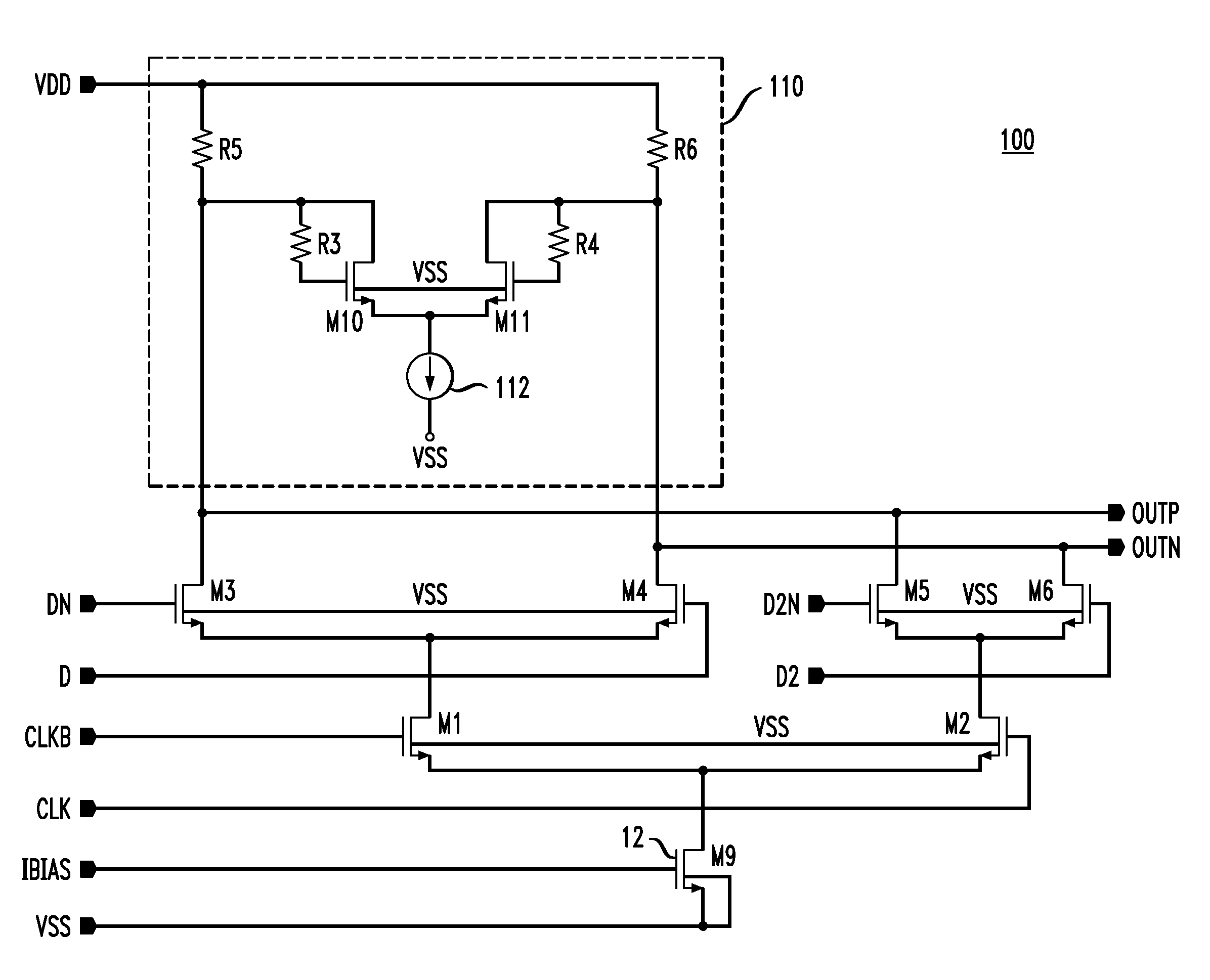
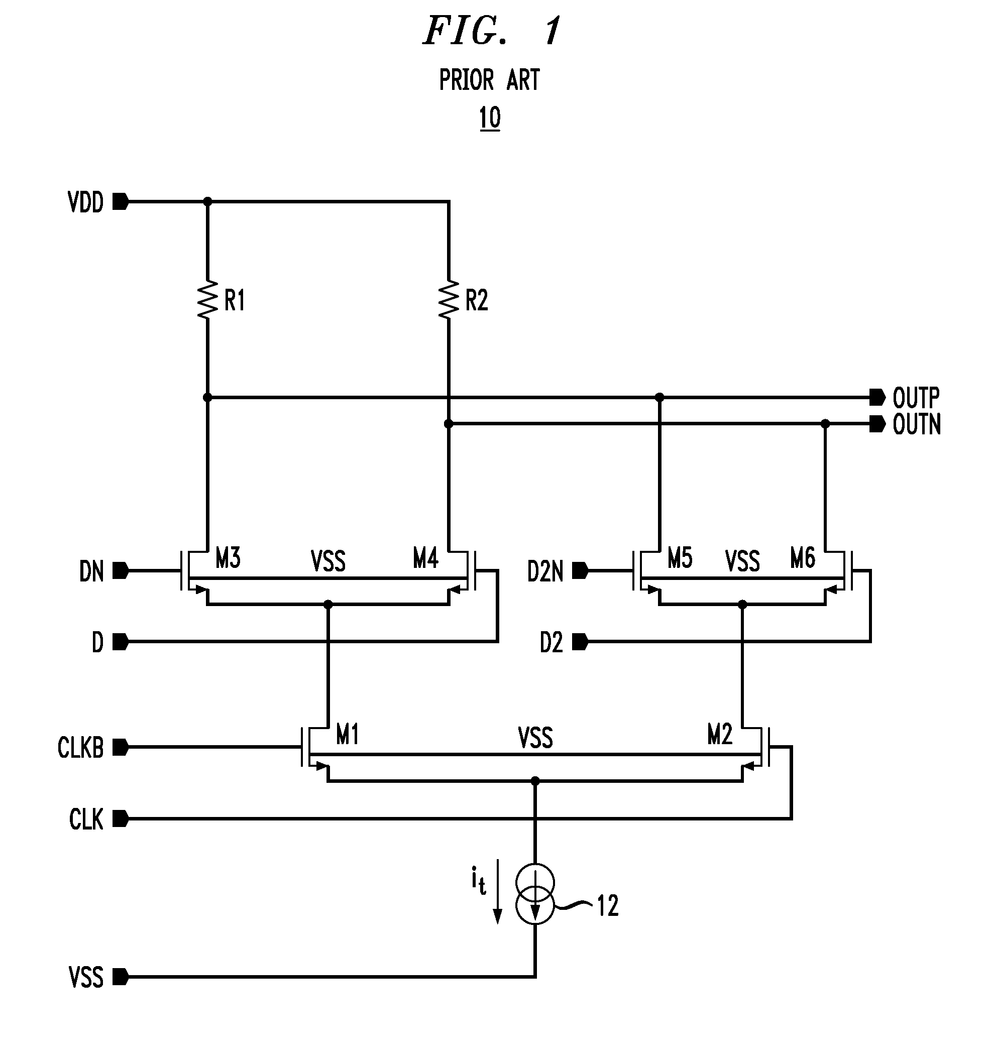
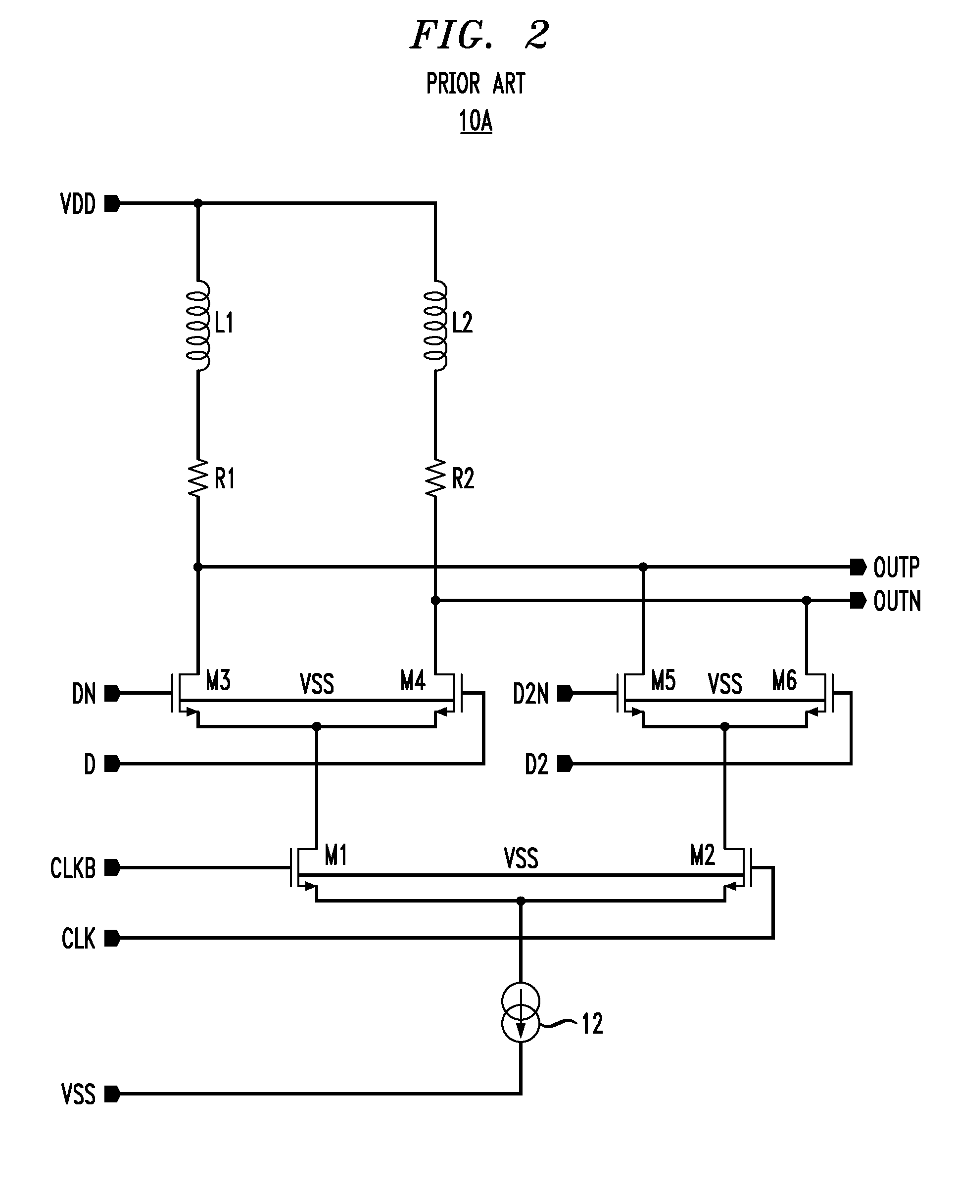
[0020]An improved inductive shunt peaking technique is described herein for enhancing the speed of CML based logic circuits. The proposed inductive shunt peaking technique can at least partially absorb or offset parasitic capacitances inherent in CML logic circuits as well as loading capacitances, thus increasing the rise / fall speed of the output signals. Specifically, folded active inductor loads are proposed for use in CML circuit designs. The technique is described herein in connection with a MOS CML data multiplexer (MUX) circuit and a MOS CML D flip-flop, but it should be understood that the loading technique is equally applicable to other CML logic circuits such as CML buffers, CML AND gates, CML OR gates, CML latches, and other CML circuits used in high speed data communication circuitry or other high speed applications. The structures of these logic circuits are not each described herein but are readily familiar to those skilled in the art of circuit design.

[0021]As those in...


PUM


Abstract

A current mode logic digital circuit is provided comprising a logic circuit component having at least one data input node and at least one output node. A load is coupled between a power supply node and the output node. The load comprises a folded active inductor coupled to the output node.

Description

CROSS-REFERENCE TO RELATED APPLICATION[0001]This application claims priority to U.S. Provisional Patent Application Ser. No. 60 / 698,375 filed Jul. 12, 2005 and entitled “Electrical Backplane Equalization Using Programmable Analog Zeros And Folded Active Inductors”, the entirety of which is hereby incorporated by reference herein.FIELD OF THE INVENTION[0002]The present invention relates generally to logic circuits and more particularly to high speed current mode logic circuits.BACKGROUND OF THE INVENTION[0003]When high-speed and low voltage swing data transfer is needed, differential signaling (also commonly referred to as double ended signals) is perhaps the most robust and promising signaling concept. Differential signaling can add an additional measure of noise immunity due to the fact that the transmitted signal is carried on two conductors and is the difference of the two signals on the two conductors. Current mode logic (CML), a design technique commonly used in high speed sign...

Claims


Application Information

Patent Timeline
Patent Type & Authority Patents(United States)
IPC IPC(8): H03K17/16H03K19/003H03K19/0175H03K19/094H03K19/20
CPCH03K19/09432H03K19/01707
Inventor CHEN, JINGHONGSHEETS, GREGORY W.SMITH, LANE A.
Owner AVAGO TECH INT SALES PTE LTD
Why Eureka
Try Eureka