Applications and fabrication techniques for large scale wire grid polarizers

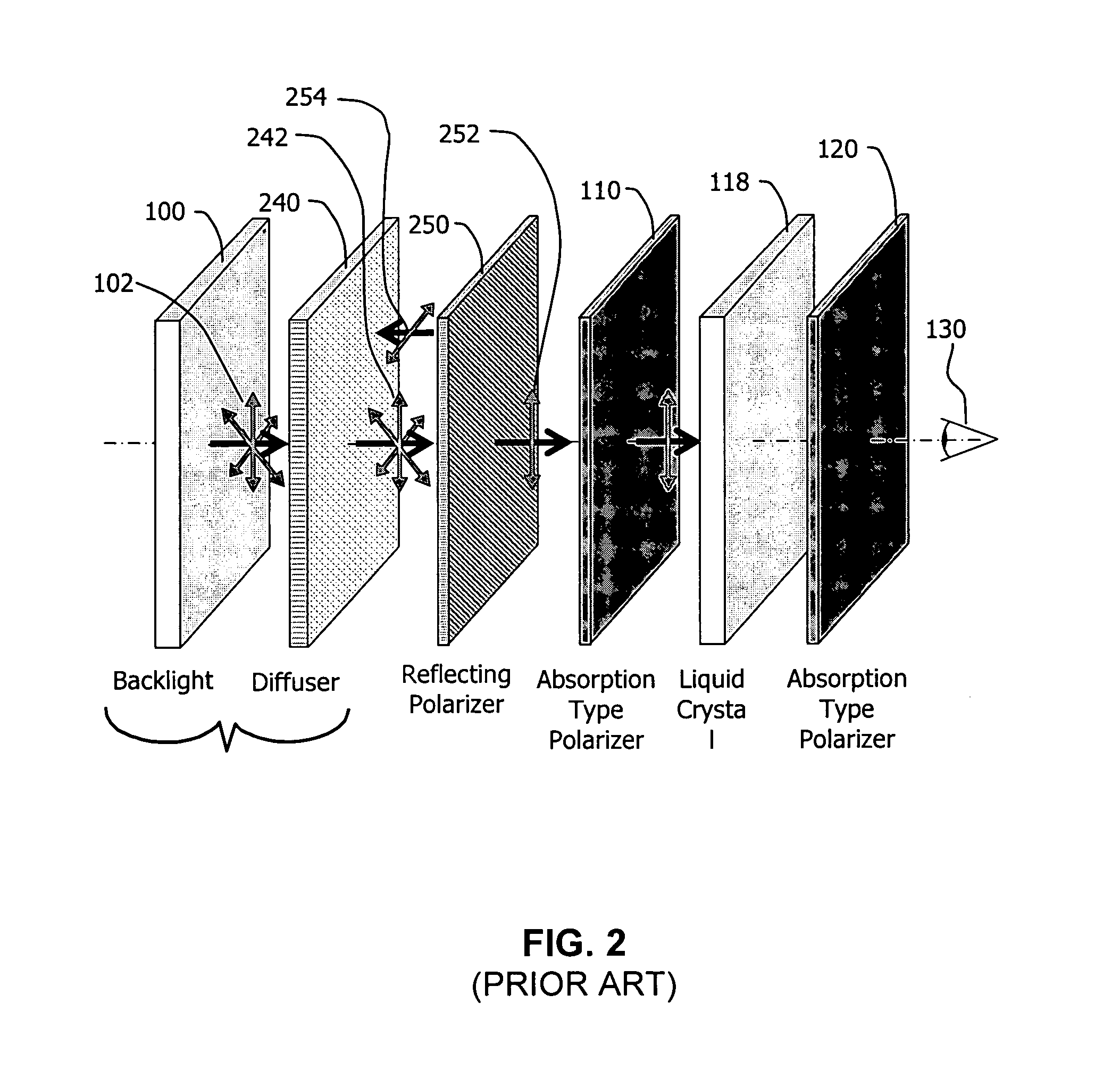
a polarizer and wire grid technology, applied in the field of wire grid polarizers, can solve the problems of poor extinction ratio of reflective polarizers, low net transmission of backlight illumination, and low efficiency of absorption-type polarizers

Inactive Publication Date: 2009-07-14
AGOURA TECH
View PDF73 Cites 65 Cited by
  • Summary
  • Abstract
  • Description
  • Claims
  • Application Information

AI Technical Summary

Problems solved by technology

One significant problem with this use of tandem absorption-type polarizers is very low net transmission of the backlight illumination.
In practice, the efficiency of the absorption-type polarizers is less than perfect and only 40-45% of the available backlight could be transmitted through any one polarizer.
The extinction ratio of reflective polarizer 250 is so poor that a second “clean-up” polarizer 110 is required for the display to produce adequate contrast; it doesn't eliminate the need for a backside absorption-type polarizer.
This is a complex and expensive manufacturing process.
In addition to the problem described above there are additional problems with these reflective polarizers that are related to both performance and cost.
Thus, while prior art reflective polarizers do address the need for improved brightness in LCDs, the above problems and other known problems remain.
As a result, wire grids having periodicities that fall within such transition region are unsuitable for use as wide band polarizers.
Wire grid polarizers operate by the reflection and transmission of light, and are therefore neither temperature sensitive nor does it absorb excessive amounts of energy.
Such temperature sensitivity limits the types of manufacturing process that may be employed to create dichroic adsorptive polarizers.
They were initially unavailable for use in the infrared and visible wavelength ranges due to the inability of then-existing processing technologies (e.g. stretching thin wires over a mandrel) to produce parallel conducting lines of sufficiently small periodicity.
Techniques for fabricating wire grid polarizers by methods employing photolithography face inherent and well-recognized limitations.
First, the lengths of the sides of the area that can be exposed during a single exposure (and, hence, the size of the polarizer) are limited to a few inches.
This is far too small for most direct view displays such as those employed in laptop computers, television sets, cell phones, personal digital assistants (PDAs) and the like.
Secondly, the cost of photolithographic processes is rather high due to the costs of high-resolution photolithography mask aligners, and the requisite ultra-high quality clean room facility required to house such a system.
A very sophisticated optical setup and lasers are needed to do this, but one can expose photoresist with the interference patterns.
However, the interference pattern that comes from interfering two oblique beams produces a periodicity that is not any smaller than the wavelength of the laser.
Thus with visible lasers it's not possible to get to the 100-nm or smaller periodicity needed for visible polarizers.
One would need an extreme ultra-violet wavelength laser and photoresists suitable for use in this spectral region are not commonly available.

Method used


Image

  • Applications and fabrication techniques for large scale wire grid polarizers
  • Applications and fabrication techniques for large scale wire grid polarizers
  • Applications and fabrication techniques for large scale wire grid polarizers

Examples


Embodiment Construction

[0038]Although the following detailed description contains many specific details for the purposes of illustration, anyone of ordinary skill in the art will appreciate that many variations and alterations to the following details are within the scope of the invention. Accordingly, the exemplary embodiments of the invention described below are set forth without any loss of generality to, and without imposing limitations upon, the claimed invention.

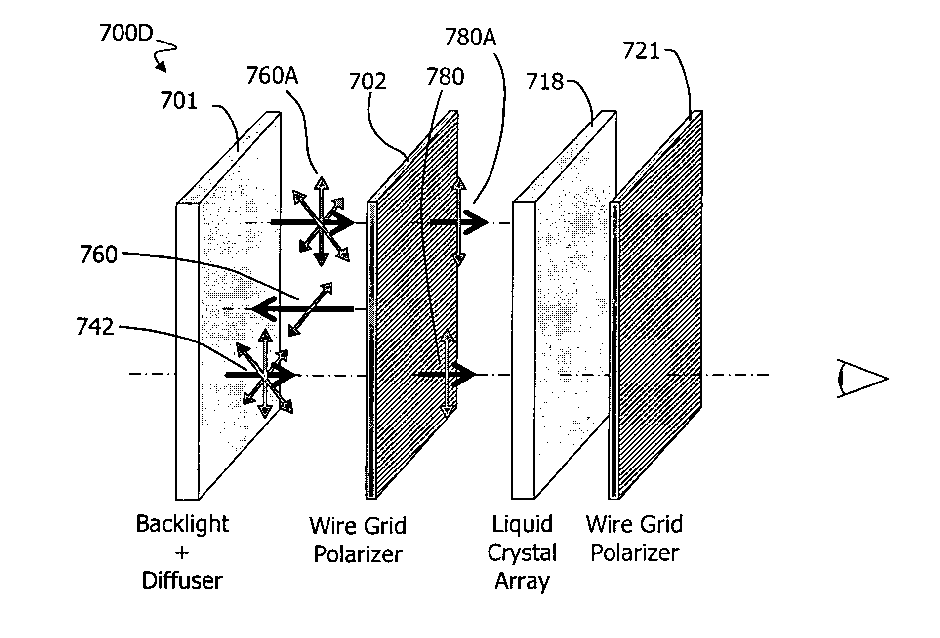
[0039]A first embodiment of the present invention provides a method for forming a wire grid polarizer characterized by parallel conductive lines of periodicities suitable for operation in the visible and infrared spectra. Unlike prior art techniques that rely upon photolithography to achieve the requisite small periodicities, the method of the present does not employ any photolithography and is therefore not subject to the resultant limitation of device size and capital equipment cost attendant to photolithographic processes. As such, large-...


PUM

PropertyMeasurementUnit
lengthaaaaaaaaaa
widthaaaaaaaaaa
lengthaaaaaaaaaa

Abstract

A wire grid polarizer may be fabricated by forming plurality of substantially-straight metallic lines of predetermined periodicity Λ on a thin film substrate A plurality of substantially straight nanometer-scale periodic surface relief structures is created on a surface of the substrate. The periodic surface relief structures cover a region greater than about 4 centimeters in length and greater than about 4 centimeters in width, wherein the periodicity Λ is between about 10 nanometers and about 500 nanometers. One or more layers of material are formed on the periodic relief structures. The one or more layers include one or more conductor materials that form the plurality of substantially straight metallic lines over a region of the substrate greater than about 4 centimeters in length and greater than about 4 centimeters in width.

Description

CROSS-REFERENCE TO RELATED APPLICATION[0001]This application claims the benefit of priority of commonly-assigned, co-pending U.S. patent application Ser. No. 11 / 001,449 filed Nov. 30, 2004 and entitled “NON-PHOTOLITHOGRAPHIC METHOD FOR FORMING A WIRE GRID POLARIZER FOR OPTICAL AND INFRARED WAVELENGTHS”, the entire disclosures of which are incorporated herein by reference. This application also claims the benefit of priority of commonly assigned U.S. provisional patent application number 60 / 677,309, filed May 4, 2005 and entitled “AN IMPROVED DIRECT-VIEW LIQUID CRYSTAL DISPLAY ASSEMBLY”, the entire disclosures of which are incorporated herein by reference. This application also claims the benefit of priority of commonly assigned U.S. provisional patent application number 60 / 677,310, filed May 4, 2005 and entitled “DIRECT-VIEW LIQUID CRYSTAL DISPLAY ASSEMBLY WITH OPTIMIZED POLARIZERS”, the entire disclosures of which are incorporated herein by reference.FIELD OF THE INVENTION[0002]Emb...

Claims


Application Information

Patent Timeline
Patent Type & Authority Patents(United States)
IPC IPC(8): G02B5/30
CPCG02B5/3058B82Y30/00C23F1/00B82Y40/00
Inventor LITTLE, MICHAEL J.MCLAUGHLIN, CHARLES W.
Owner AGOURA TECH
Why Eureka
Try Eureka