Semiconductor device including a lateral field-effect transistor and Schottky diode

a field-effect transistor and diode technology, applied in semiconductor devices, diodes, electrical apparatus, etc., can solve the problems of reducing the applicability of the device in certain situations, unable to accommodate a careful doping profiling, and unable to meet the requirements of careful doping profiling, so as to achieve low resistance coupling

Active Publication Date: 2009-07-21
MYPAQ HLDG LTD
View PDF92 Cites 14 Cited by
  • Summary
  • Abstract
  • Description
  • Claims
  • Application Information

AI Technical Summary

Problems solved by technology

The field-effect transistor as described above, however, does not accommodate a careful doping profiling and epitaxial layer design necessary to produce a modulation-doped channel that can be formed in a lateral channel and that may be employed to substantially reduce the on-resistance of the device.
The structure as generally described in the aforementioned references has higher channel and gate resistance per unit die area than the desired resistance and produces a device operable only in the depletion mode, which may limit the applicability of the device in certain situations.
The resulting cost and performance have resulted in limited marketability in view of the presently available silicon-based technology.
Although economies of manufacture are achieved using implants rather than etching and epitaxial growth as described by Eisenbeiser, et al., possible disadvantages of a channel with a vertical structure limit the switching speed and operation as an enhancement-mode device.
Designing the source and drain contacts on the same surface of the die requires a complicated multilayer metallization process and results in increased die area and reduced chip yield.
Although this arrangement can provide low-inductance external connections to the source, it is limited in its ability to provide a low-resistance channel tightly coupled to the lower surface of a highly conductive substrate, or an intrinsic body diode.
The aforementioned design also does not accommodate large drain contacts desirable for a higher power device, which will increase the resistive and inductive losses.
This configuration requires a complex air-bridge processing step, which will increase the cost and potentially affect the reliability of the device.
This design also is incompatible with today's packaging techniques for higher power devices embodied in a vertical device configuration.
The aforementioned devices, however, are configured with contacts on a top surface, which restricts their application from low voltage, high current systems wherein efficiency is an important design element.
While a Schottky diode may be employed in parallel with the active switching device, typically the Schottky diode adds cost to the circuit and requires valuable space for the circuit implementation.
The presence of a p-n-based diode generally results in switching losses due to forward and reverse recovery phenomena.
These loss mechanisms result, respectively, in increased forward voltage drop immediately after a diode is turned on, and a reverse current flow immediately after a diode is turned off.
Considering the limitations as described above, a field-effect transistor design is not presently available for the more severe applications that lie ahead.

Method used


Image

  • Semiconductor device including a lateral field-effect transistor and Schottky diode
  • Semiconductor device including a lateral field-effect transistor and Schottky diode
  • Semiconductor device including a lateral field-effect transistor and Schottky diode

Examples


Embodiment Construction

[0030]The making and using of the presently preferred embodiments are discussed in detail below. It should be appreciated, however, that the present invention provides many applicable inventive concepts that can be embodied in a wide variety of specific contexts. The specific embodiments discussed are merely illustrative of specific ways to make and use the invention, and do not limit the scope of the invention.

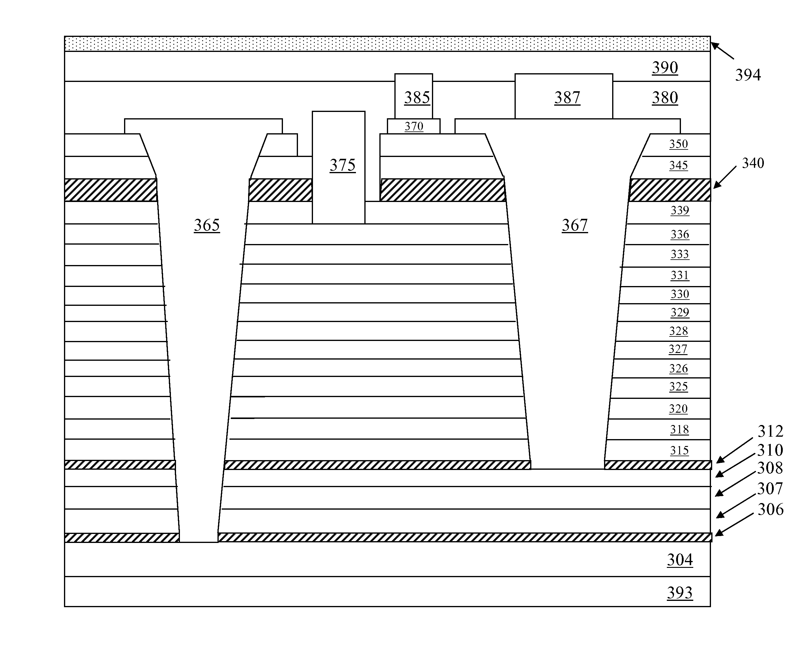
[0031]The present invention will be described with respect to exemplary embodiments in a specific context, namely, a semiconductor device and, more particularly, a semiconductor device having a lateral field-effect transistor (“FET”) and a Schottky diode formed on the same die, coupled to drain and source contacts thereof. The lateral FET includes a source contact coupled to a doped epitaxial buffer layer formed on a substrate, which can be optionally removed during device processing to reduce device electrical and thermal resistances. A drain contact is coupled to an opposin...


PUM


Abstract

A semiconductor device including a lateral field-effect transistor and Schottky diode and method of forming the same. In one embodiment, the lateral field-effect transistor includes a buffer layer having a contact covering a substantial portion of a bottom surface thereof, a lateral channel above the buffer layer, another contact above the lateral channel, and an interconnect that connects the lateral channel to the buffer layer. The semiconductor device also includes a Schottky diode parallel-coupled to the lateral field-effect transistor including a cathode formed from another buffer layer interposed between the buffer layer and the lateral channel, a Schottky interconnect interposed between the another buffer layer and the another contact, and an anode formed on a surface of the Schottky interconnect operable to connect the anode to the another contact. The semiconductor device may also include an isolation layer interposed between the buffer layer and the lateral channel.

Description

[0001]This application is a continuation in part of, and claims priority to, U.S. patent application Ser. No. 11 / 211,964, entitled “Semiconductor Device Having Substrate-Driven Field-Effect Transistor and Schottky Diode and Method of Forming the Same,” filed on Aug. 25, 2005, now U.S. Pat. No. 7,285,807, issued Oct. 23, 2007, which is incorporated herein by reference.TECHNICAL FIELD[0002]The present invention is directed, in general, to semiconductor devices and, more specifically, to a semiconductor device including a field-effect transistor with at least one lateral channel and a Schottky diode, and a method of forming the same.BACKGROUND[0003]A field-effect transistor (also referred to as a “FET”) is a conventional semiconductor device employable in switch-mode power supplies for use in data processing and telecommunication systems as well as for other applications that use conditioned power for the operation of sensitive electronic circuits. Field-effect transistors have almost ...

Claims


Application Information

Patent Timeline
Patent Type & Authority Patents(United States)
IPC IPC(8): H01L31/0328
CPCH01L27/0605H01L27/0629H01L29/872H01L29/66462H01L29/7783H01L27/0727H01L29/20
Inventor SADAKA, MARIAM GERGIBRAR, BERINDER P. S.HA, WONILLNGUYEN, CHANH NGOC MINH
Owner MYPAQ HLDG LTD
Why Eureka
Try Eureka