Content addressable memory (CAM) device and method for flexible suppression of hit indications
- Summary
- Abstract
- Description
- Claims
- Application Information
AI Technical Summary
Benefits of technology
Problems solved by technology
Method used
Image
Examples
first embodiment
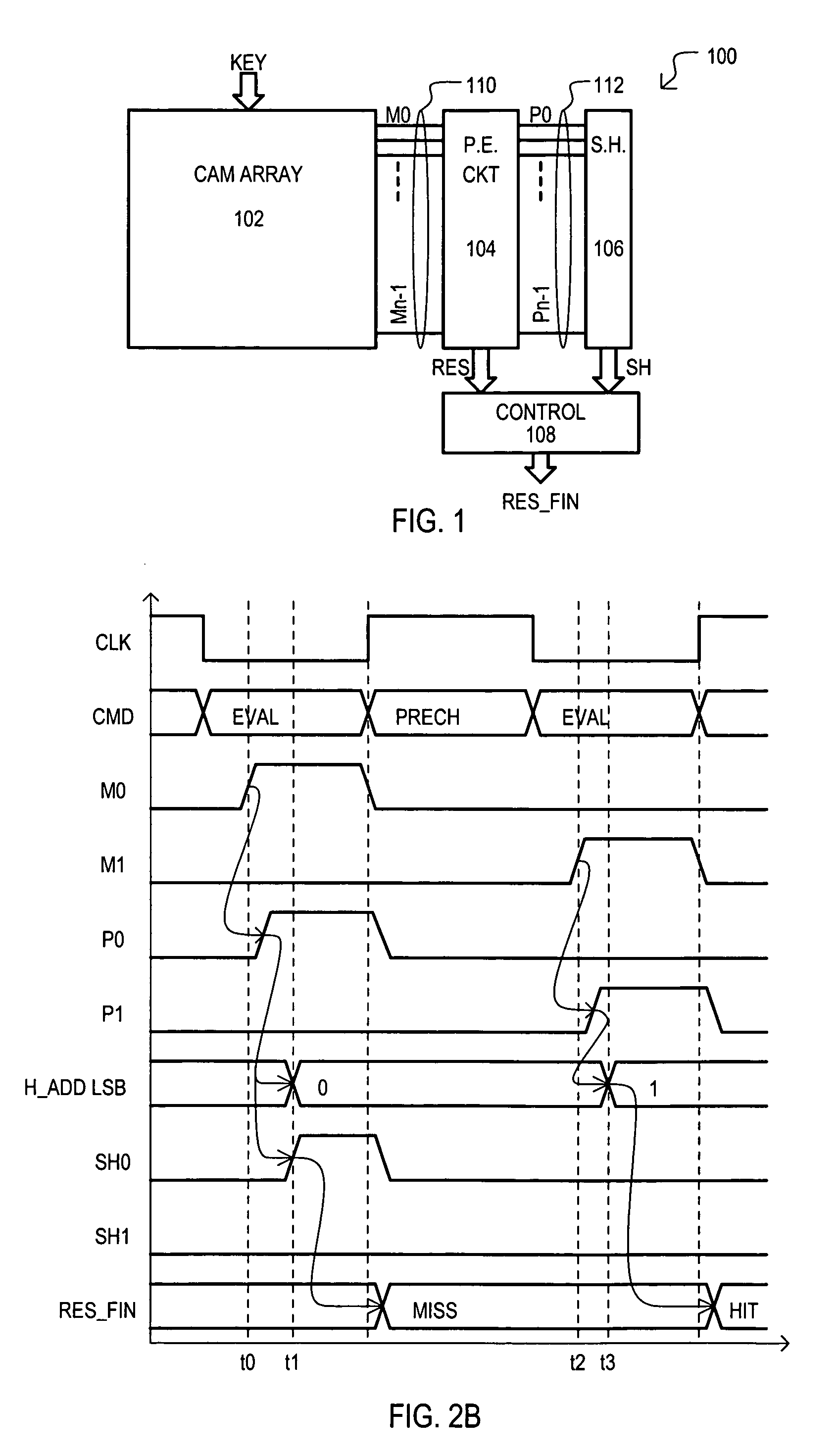
[0050]Referring now to FIG. 1, a CAM device is set forth in a block schematic diagram and designated by the general reference character 100. A CAM device 100 can include a CAM cell array 102, a priority encoder section 104, a suppression data store 106, and a control circuit 108. A CAM cell array 102 can have a number of CAM entries that can compare stored data values with an applied key KEY in a search operation. Each entry can provide match indications (M0 to Mn−1) on corresponding match lines 110. As but one example, each entry can include a row of CAM cells commonly connected to a match line.
[0051]A priority encoder circuit 104 can prioritize generated match indications M0 to Mn−1 according to predetermined criteria to activate one priority encoder output signal P0 to Pn−1. Such a single activated signal can be considered to correspond to a “winning” CAM entry. Priority encoder output signals (P0 to Pn−1) can be provided on corresponding priority encoder output lines 112. In on...
second embodiment
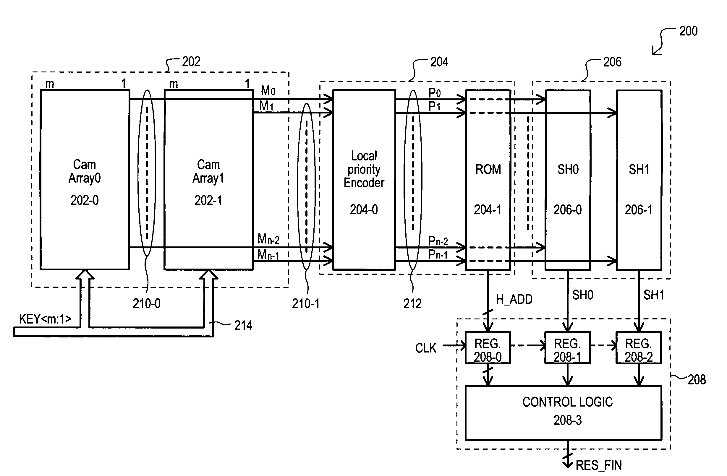
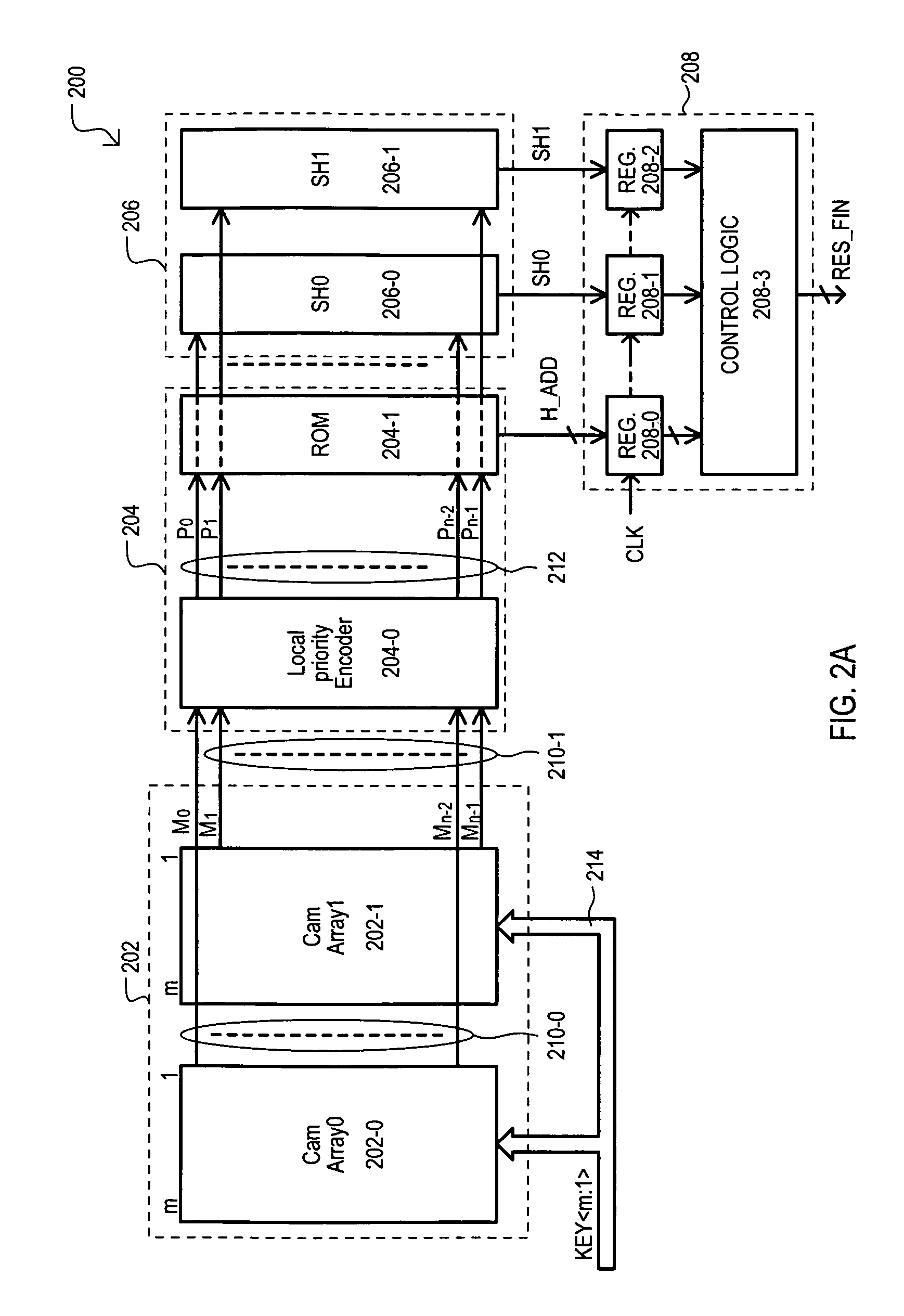
[0056]the present invention will now be described with reference to FIG. 2A.
[0057]FIG. 2A is a schematic diagram of a CAM device 200 that includes some of the same general components as FIG. 1. Accordingly, like component will be referred to by the same reference character but with the first digit being a “2” instead of a “1”.
[0058]In the arrangement of FIG. 2A, a memory cell array 202 can include a first CAM array 202-0 and a second CAM array 202-1, each of which contains a number of CAM entries. In the very particular example of FIG. 2A, both first and second CAM arrays (202-0 and 202-1) can include “n / 2” CAM entries total, each of which can generate a match indication on a corresponding match line (M0 to Mn−1). Further, CAM entries in a first CAM array 202-0 can correspond to even physical addresses, and thus possess address having a least significant bit of “0”. CAM entries in a second CAM array 202-1 can correspond to odd physical addresses, and thus possess address having a le...
third embodiment
[0078]the present invention will now be described with reference to FIG. 3A.
[0079]FIG. 3A is a schematic diagram of a CAM device 300 that includes similar components as FIG. 2. Accordingly, like components will be referred to by the same reference character but with the first digit being a “3” instead of a “2”.
[0080]A CAM device 300 can differ from that of FIG. 2A in that match results from different CAM arrays 302-0 and 302-1 can be logically combined to generate a result for a wider word than native word size (more than “m” bits, in this example). In the very particular example of FIG. 3A, a logic circuit 316 can logically combine one match line from each CAM array 302-0 to generate combined match results (M0 to M(n−2) / 2) on combined result lines 318. As a result, the number of combined results values is n / 2.
[0081]In this way, a CAM device 300 can provide suppression for matches based on data words having a greater size than a native word for the device (a native word being the wi...
PUM
 Abstract
Description
Claims
Application Information


