Method for forming an electronic device in multi-layer structure

a technology of electronic devices and layers, applied in the field of electronic devices, can solve the problems of many direct printing techniques not being able to provide patterning resolution

Inactive Publication Date: 2009-08-11
CAMBRIDGE UNIV TECHNICAL SERCICES LTD +2
View PDF27 Cites 37 Cited by
  • Summary
  • Abstract
  • Description
  • Claims
  • Application Information

AI Technical Summary

Benefits of technology

[0009]Other aspects of the invention include devices formed by that and other methods, and integrated circuits, logic circuits, display circuits and/or memory device circuits com

Problems solved by technology

Many direct printing techniques are unable to provide the patterning resol

Method used


Image

  • Method for forming an electronic device in multi-layer structure
  • Method for forming an electronic device in multi-layer structure
  • Method for forming an electronic device in multi-layer structure

Examples


Embodiment Construction

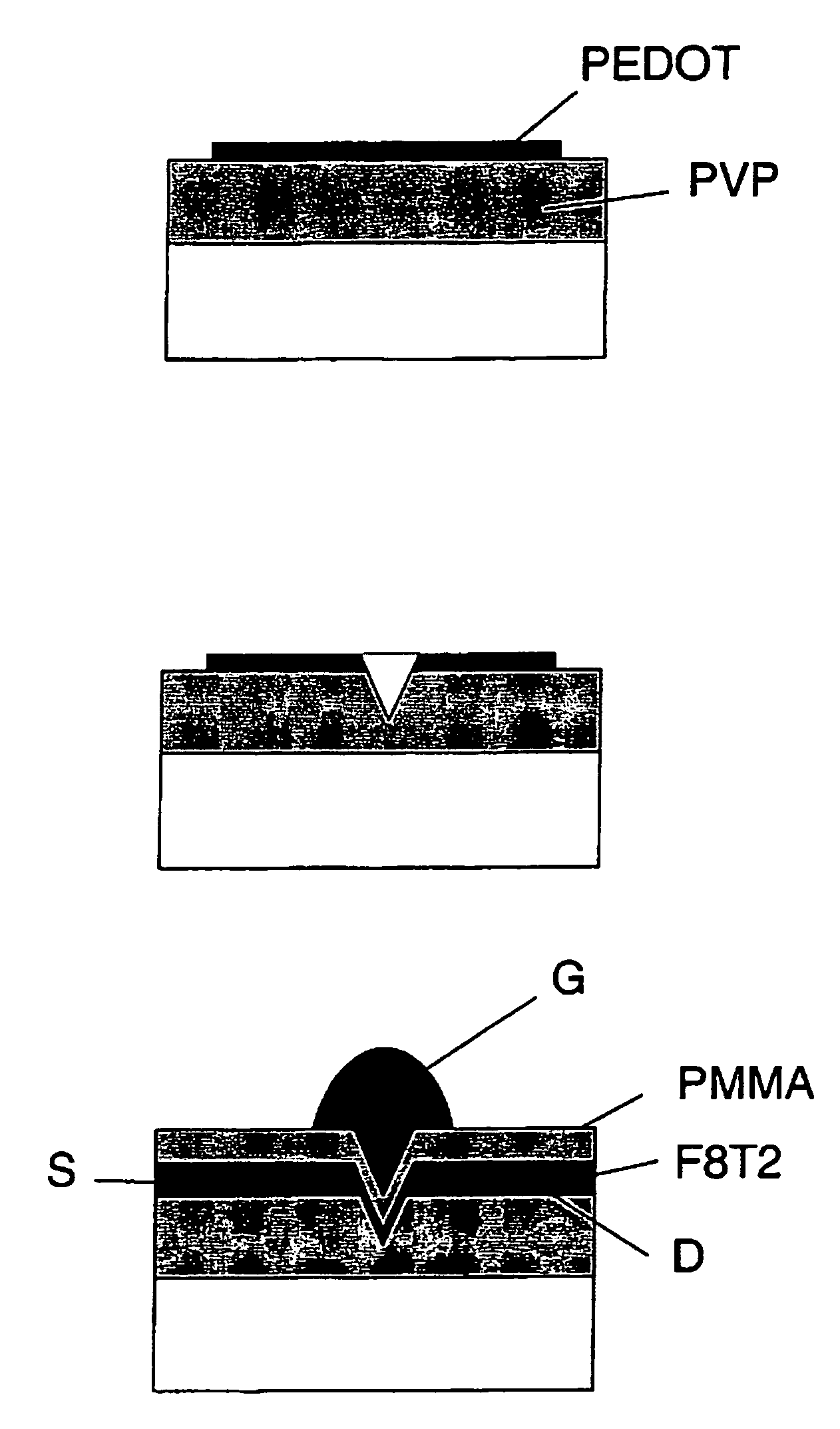
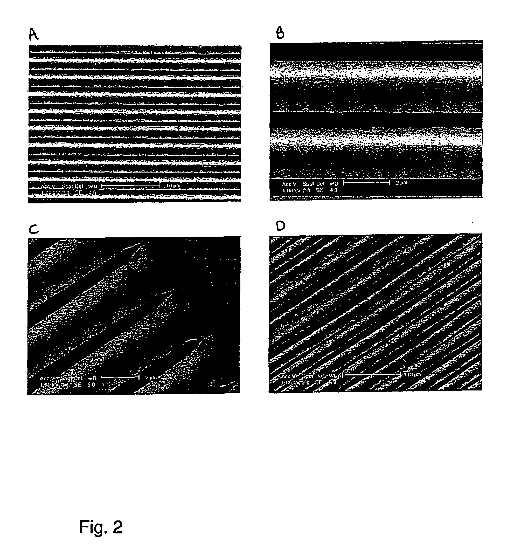
[0028]A first example demonstrates the application of solid state embossing to microcutting of conducting polymer films.

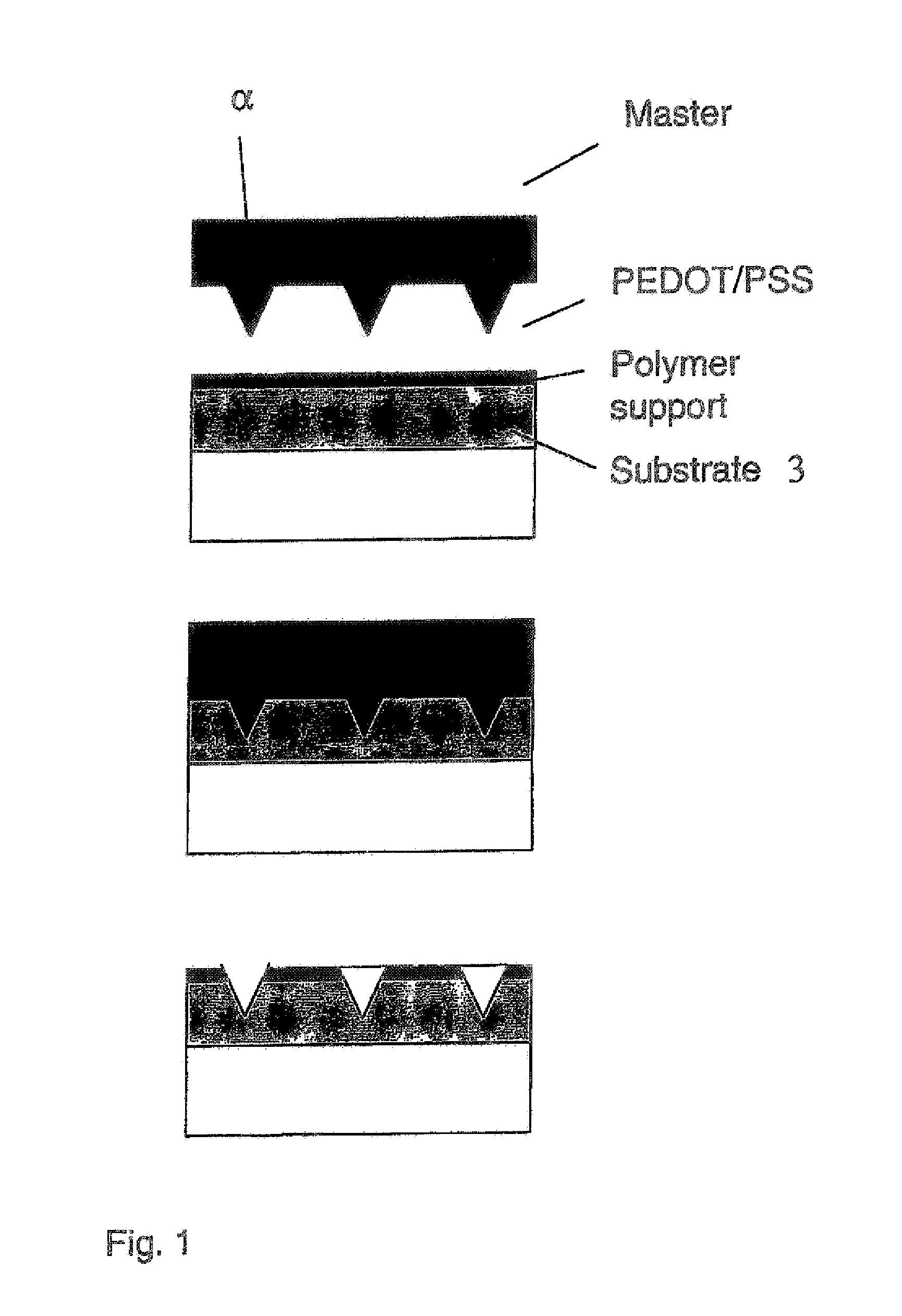
[0029]FIG. 1 shows a schematic diagram of solid state embossing of a thin film of PEDOT / PSS on top of a thick, smooth insulating polymer support such as PMMA, poly(vinylphenol) (PVP), poly(styrene) (PS) or polyimide (PI). The insulating polymer film is deposited on top of the 7059 glass substrate by spin coating from a 15-30 weight % solution in propylene glycol methyl ether acetate (PVP) and cyclopentanone (PMMA), respectively, resulting in a film thickness of 2-3 μm. Prior to the deposition of the PEDOT the surface of the insulating polymer is rendered hydrophilic by O2 plasma treatment in order to promote the adhesion of the PEDOT film. A 800 Å film of PEDOT / PSS (Baytron P from Bayer corporation) is then spincoated from a water dispersion. Embossing is performed at a temperature of 150° C. (PVP), 100° C. (PS), 105° C. (PMMA) for up to 60 min with a load of about...


PUM

PropertyMeasurementUnit
Temperatureaaaaaaaaaa
Radiusaaaaaaaaaa
Radiusaaaaaaaaaa

Abstract

A method for forming an organic or partly organic switching device, comprising: depositing layers of conducting, semiconducting and/or insulating layers by solution processing and direct printing; defining microgrooves in the multilayer structure by solid state embossing; and forming a switching device inside the microgroove.

Description

BACKGROUND OF THE INVENTION[0001]1. Field of the Invention[0002]This invention relates to electronic devices, especially organic electronic devices, and methods for forming such devices.[0003]2. Description of the Related Art[0004]Semiconducting conjugated polymer thin-film transistors (TFTs) have recently become of interest for applications in cheap, logic circuits integrated on plastic substrates (C; Drury, et al., APL 73, 108 (1998)) and optoelectronic integrated devices and pixel transistor switches in high-resolution active-matrix displays (H. Sirringhaus, et al., Science 280, 1741 (1998), A. Dodabalapur, et al. Appl. Phys. Left. 73, 142 (1998)). In test device configurations with a polymer semiconductor and inorganic metal electrodes and gate dielectric layers high-performance TFTs have been demonstrated. Charge carrier mobilities up to 0.1 cm2Ns and ON-OFF current ratios of 106-108 have been reached, which is comparable to the performance of amorphous silicon TFTs (H. Sirring...

Claims


Application Information

Patent Timeline
IPC IPC(8): B23P17/00B81C99/00H01L21/336H01L27/28H01L29/12H01L29/78H01L29/786H01L51/00H01L51/05H01L51/30H01L51/40
CPCB82Y30/00H01L51/0014H01L51/0022H01L51/0508H01L51/055Y10T29/49126H01L51/0005H01L51/0037H01L51/0039H01L51/057H01L2251/105Y10T29/49798Y10T29/4913Y10T29/49128Y10T29/14Y10T29/49117H01L27/283H10K19/10H10K71/135H10K71/20H10K71/611H10K85/115H10K85/1135H10K10/46H10K10/481H10K10/491H10K71/821H01L29/786
Inventor SIRRINGHAUS, HENNINGFRIEND, RICHARD HENRYSTUTZMANN, NATALIESMITH, PAUL
Owner CAMBRIDGE UNIV TECHNICAL SERCICES LTD
Why Eureka
Try Eureka