Check patentability & draft patents in minutes with Patsnap Eureka AI!

Clock multiplier structure for fixed speed testing of integrated circuits

a multiplier circuit and integrated circuit technology, applied in oscillation generators, generating/distributing signals, pulse techniques, etc., can solve the problems of increasing the difficulty of cost-effectively testing high-speed memories, requiring a relatively significant amount of space on the chip of internal plls, and reducing the efficiency of internal plls

Inactive Publication Date: 2009-08-18
IBM CORP
View PDF11 Cites 8 Cited by
  • Summary
  • Abstract
  • Description
  • Claims
  • Application Information

AI Technical Summary

Benefits of technology

The patent text describes a clock multiplier structure for testing integrated circuits. The structure includes a clock signal generator with a ring oscillator and a rollover counter. The ring oscillator generates an oscillator signal with multiple cycles, and the rollover counter counts the cycles from a seed value to a terminal value and outputs a pulse each time it reaches the first terminal value. The saturation counter counts the cycles from a multiplier start value to a saturation value and outputs a binary signal indicating whether it has reached the saturation value. The seed value generator generates the seed value when the binary signal indicates that the saturation has not reached the saturation value. The integrated circuit also includes functional circuitry that receives the first clock signal. The technical effect of this structure is to provide a reliable and accurate clock signal for testing integrated circuits.

Problems solved by technology

Dynamic random access memory (DRAM) circuits and devices are frequently subject to burn-in testing.
As memory speeds become higher with successive generations of technology, the ability to cost-effectively test these high-speed memories is becoming more difficult due to, for example, the need for high-speed test clocks to properly exercise the memory during burn-in.
However, internal PLLs require a relatively significant amount of space on a chip, have relatively high power requirements, and have no means for efficiently dealing with very long tester cycles since it will generally require a delay mechanism that would clone the tester cycle and require unique devices, such as resistors, capacitors, low leakage and high threshold devices.

Method used


Image

  • Clock multiplier structure for fixed speed testing of integrated circuits
  • Clock multiplier structure for fixed speed testing of integrated circuits
  • Clock multiplier structure for fixed speed testing of integrated circuits

Examples


Embodiment Construction

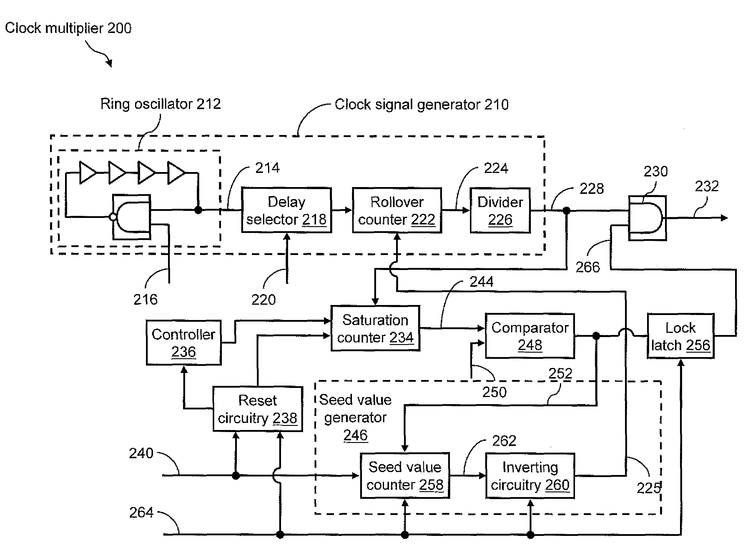
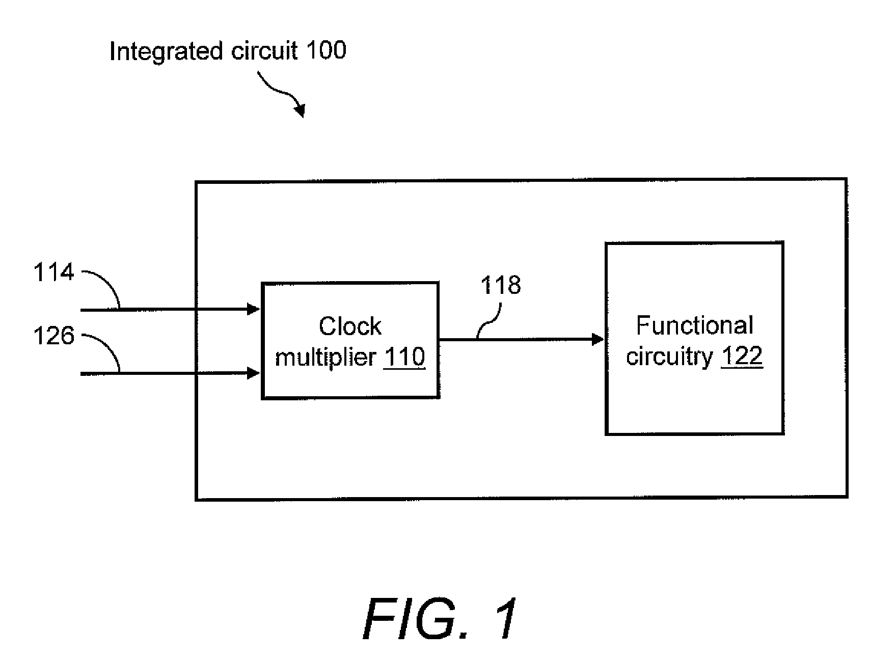
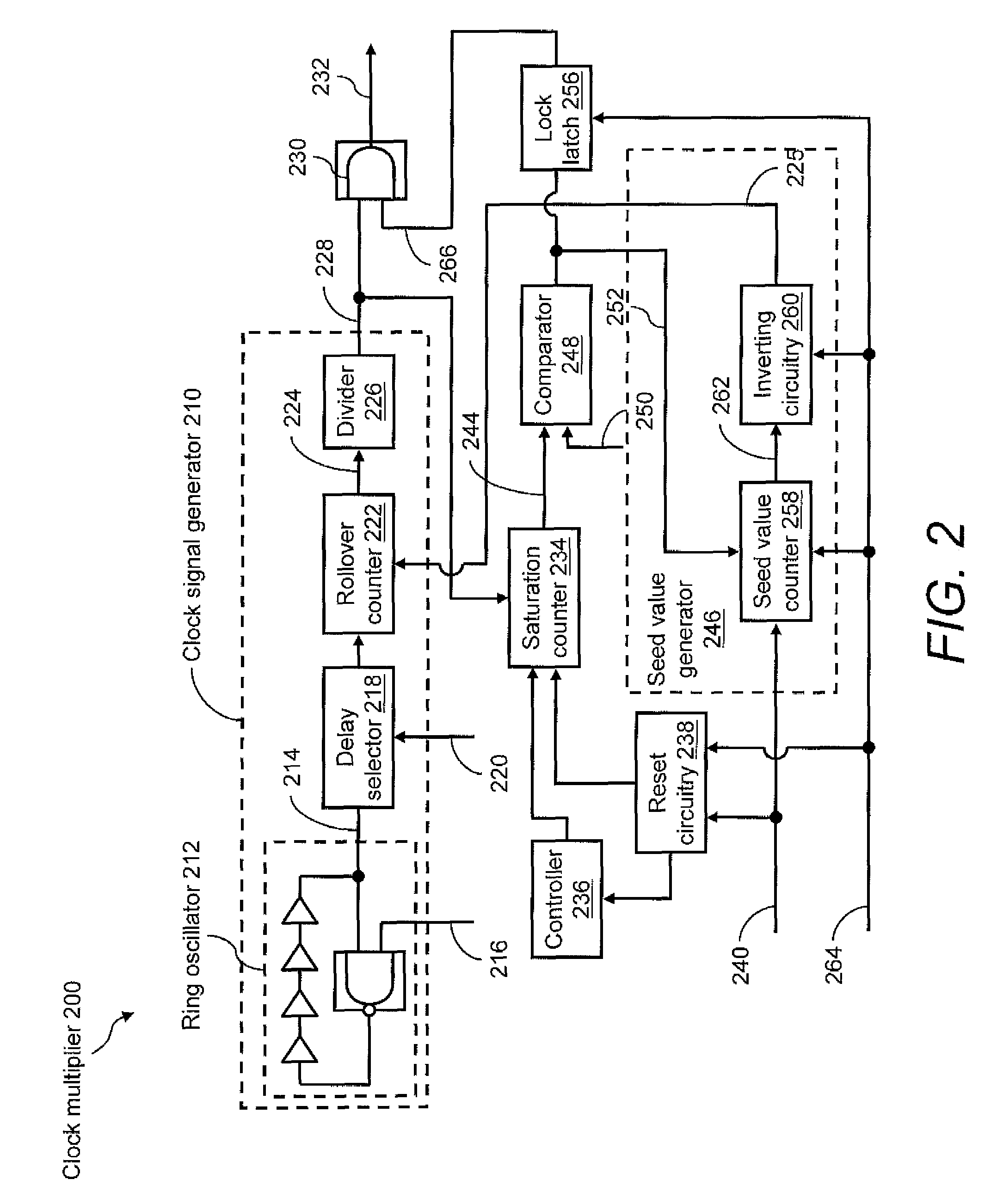
[0010]FIG. 1 illustrates an integrated circuit 100 that includes a clock multiplier 110 for generating a fast clock from a slow clock. Clock multiplier 110 is fed by an input clock signal to be multiplied, such as test clock signal 114, and provides an output clock signal 118 having a frequency greater than the frequency of test clock signal 114 by a certain predetermined multiple, which may be fixed or programmable. Output clock signal 118 may be provided to functional circuitry 122, which may be any suitable functional circuitry, such as one or more dynamic random access memories (DRAMs), SRAMS, Memory BISTs, application specific circuits, etc.

[0011]In two examples, the multiplier is 32 and 8, respectively. The first example may be pertinent, for example, to a burn-in test that requires the output clock signal 118 to have a period no greater than 20 ns but where the test cycle time is about 300 ns, i.e., the frequency of test clock signal 114 is about 333 kHz. Such a burn-in test ...


PUM


Abstract

An on-chip clock multiplier for outputting a fast clock that is approximately a predetermined multiple n of a slow clock. The multiplier utilizing a high-speed oscillator to generate a high-frequency base signal. A lower frequency signal is generated using the high-frequency base signal as a function of the output of a rollover counter that counts from a seed value to a terminal value. A saturation counter is used to determine whether no more than n pulses of the lower frequency signal occur within a single cycle of the slow clock. If not, the lower frequency signal is iteratively slowed by changing the seed value until no more than n pulses of the lower frequency signal occur within a single cycle of the slow clock. When this iteration is done, the fast clock having a frequency that is approximately n times the frequency of the slow clock is output.

Description

FIELD OF THE DISCLOSURE[0001]The present disclosure generally relates to the field of clock generator circuits. In particular, the present disclosure is directed to a small scale clock multiplier circuit for fixed speed testing.BACKGROUND[0002]Integrated circuits are subjected to various sorts of tests depending on the capabilities and requirements of the device under test. One such test is a “burn-in” test, which is the process of exercising an integrated circuit at elevated voltage and temperature in attempt to cause the circuit to quickly fail under high-stress conditions if particular defects are present in the device. Dynamic random access memory (DRAM) circuits and devices are frequently subject to burn-in testing. As memory speeds become higher with successive generations of technology, the ability to cost-effectively test these high-speed memories is becoming more difficult due to, for example, the need for high-speed test clocks to properly exercise the memory during burn-i...

Claims


Application Information

Patent Timeline
Patent Type & Authority Patents(United States)
IPC IPC(8): H03K21/00
CPCG06F7/68G06F1/08
Inventor POMICHTER, JR., GERALD P.
Owner IBM CORP
Features
  • R&D
  • Intellectual Property
  • Life Sciences
  • Materials
  • Tech Scout
  • Unparalleled Data Quality
  • Higher Quality Content
  • 60% Fewer Hallucinations
Learn More