Method of fabricating complementary metal-oxide-semiconductor transistor and metal-oxide-semiconductor transistor

a technology of metal-oxide-semiconductor and metal-oxide-semiconductor, which is applied in the manufacturing of semiconductor/solid-state devices, basic electric elements, electric devices, etc., can solve the problems of device electrical properties, device hardly operating normally, and diffusion regions in the ldd structure of the device may be either too large or too small

Active Publication Date: 2009-09-01
UNITED MICROELECTRONICS CORP
View PDF8 Cites 0 Cited by
  • Summary
  • Abstract
  • Description
  • Claims
  • Application Information

AI Technical Summary

Benefits of technology

[0009]Accordingly, at least one objective of the present invention is to provide a method of fabricating a metal-oxide-semiconductor (MOS) transistor capable of producing lightly doped drain (LDD) structures for devices having different dimensions so that the production of too large or too small diffusion regions in the LDD structures of different size devices, which may lead to possible problems such as short channel effect or punch through and deterioration of the electrical properties of the device with consequential degradation of device performance, can be avoided.
[0010]Another objective of the present invention is to provide a method of fabricating a complementary metal-oxide-semiconductor (CMOS) transistor capable of producing lightly doped drain (LDD) structures for devices having different dimensions so that the production of too large or too small diffusion regions in the LDD structures of different size devices and related problems can be avoided.
[0011]Yet another objective of the present invention is to provide a method of fabricating a complementary metal-oxide-semiconductor (CMOS) transistor similarly capable of producing lightly doped drain (LDD) structures for devices having different dimensions so that the production of too large or too small diffusion regions in the LDD structures of different size devices and related problems can be avoided.
[0032]In the present invention, the process of fabricating the lightly doped drain structure of larger devices is carried out first, then the lightly doped drain regions are annealed and finally the process of fabricating the lightly doped drain structure of smaller devices is carried out. Thus, too much lateral diffusion in smaller devices leading to short channel effect or punch through problems and too little lateral diffusion in larger devices leading to a high impedance in the overlapping region between the lightly doped drain region and the gate, thereby lowering the saturation and drain current and affecting device performance, can be avoided. In addition, the source / drain annealing process includes a mini-second annealing process so that the temperature rise and fall within a very short time interval. Therefore, excessive diffusion within the doped regions (including the source / drain regions and the lightly doped drain regions) is prevented.

Problems solved by technology

The short channel effect and hot carrier effect is so devastating that the device can hardly operate normally.
Otherwise, the diffusion regions in the LDD structures of the devices may be either too large or too small due to their different sizes.
An inappropriately fabricated diffusion region in the LDD structure may affect the electrical properties of the device and lead to device failure.
In particular, since the dimension of each device is already so small, too much lateral diffusion will lead to short channel effect or punch through problems.
On the other hand, for larger devices, too little lateral diffusion will lead to a high impedance at the overlapping region between the LDD and the gate, thereby lowering the saturated drain current and affecting the performance of the device.

Method used


Image

  • Method of fabricating complementary metal-oxide-semiconductor transistor and metal-oxide-semiconductor transistor
  • Method of fabricating complementary metal-oxide-semiconductor transistor and metal-oxide-semiconductor transistor
  • Method of fabricating complementary metal-oxide-semiconductor transistor and metal-oxide-semiconductor transistor

Examples


Embodiment Construction

[0038]Reference will now be made in detail to the present preferred embodiments of the invention, examples of which are illustrated in the accompanying drawings. Wherever possible, the same reference numbers are used in the drawings and the description to refer to the same or like parts.

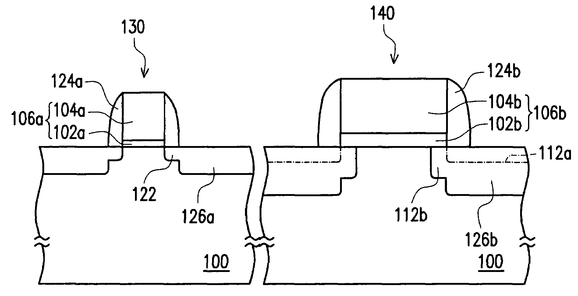
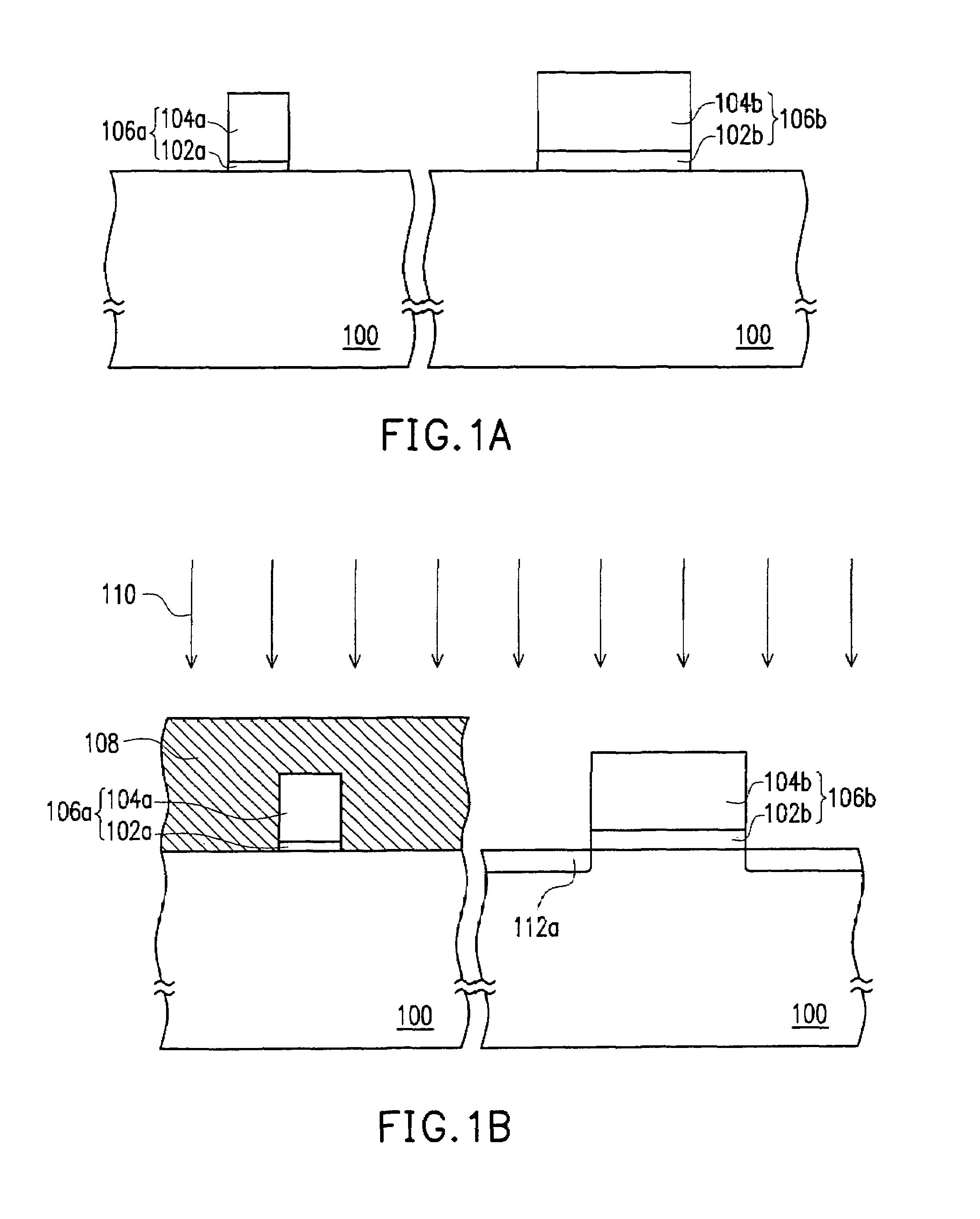
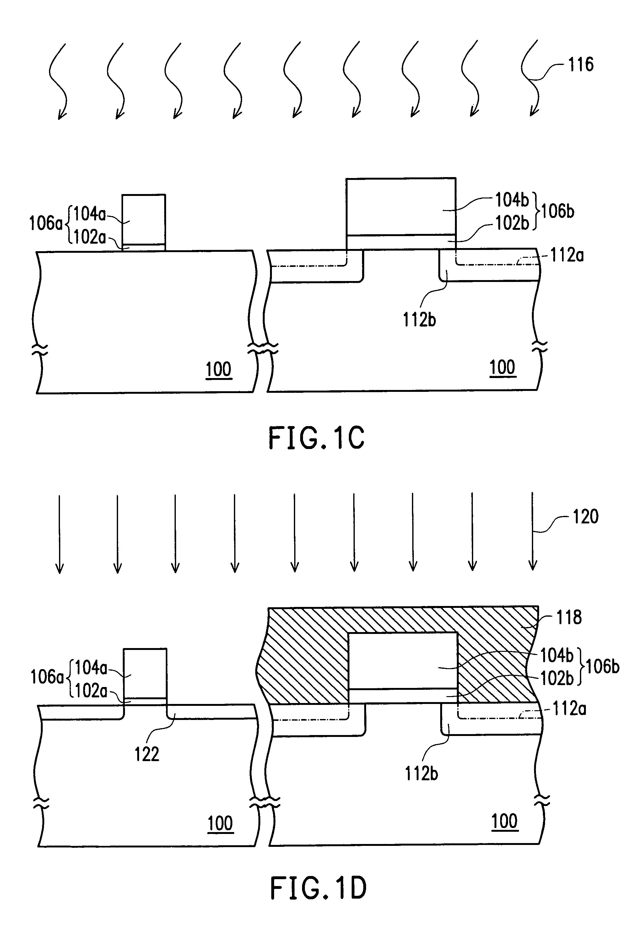
[0039]FIGS. 1A through 1F are schematic cross-sectional views showing the steps for fabricating a metal-oxide-semiconductor (MOS) transistor according to one embodiment of the present invention. In the present embodiment, an N-type transistor is used as an example. However, the applications of the present invention are not limited as such. In practice, the present invention can be applied to a P-type transistor after some adjustments and modifications.

[0040]As shown in FIG. 1A, a substrate 100 is provided. The substrate 100 can be a conventional silicon substrate or an SOI (silicon on insulator) type substrate. Then, gate dielectric layers 102a and 102b are formed on the substrate 100. The material f...


PUM


Abstract

A method of fabricating a metal-oxide-semiconductor transistor is provided. A first gate structure and a second gate structure are formed on a substrate. The first gate structure has a dimension greater than the second gate structure. Then, first lightly doped drain regions are formed in the substrate on two sides of the first gate structure. A lightly doped drain annealing process is performed. Next, second lightly doped drain regions are formed in the substrate on two sides of the second gate structure. First spacers are formed on the sidewalls of the first gate structure and second spacers are formed on the sidewalls of the second gate structure at the same time. Afterwards, first source / drain regions are formed in the substrate on two sides of the first spacers and second source / drain regions are formed in the substrate on two sides of the second spacers. A source / drain annealing process is performed.

Description

BACKGROUND OF THE INVENTION[0001]1. Field of the Invention[0002]The present invention relates to a method of fabricating integrated circuit device, and more particularly, to a method of fabricating a complementary metal-oxide-semiconductor (CMOS) transistor and a metal-oxide-semiconductor (MOS) transistor.[0003]2. Description of Related Art[0004]Metal-oxide-semiconductor (MOS) transistor is a basic device in logic circuits. Each transistor comprises a gate, a source / drain (S / D) region in the substrate on two sides of the gate, and a channel between the source region and the drain region. When the manufacturing of MOS transistor is progressed into the micrometer level, short channel effect and hot carrier effect is intensified due to the shortening of the channel between source / drain regions. The short channel effect and hot carrier effect is so devastating that the device can hardly operate normally. Therefore, a lightly doped drain (LDD) structure is often introduced into the desig...

Claims


Application Information

Patent Timeline
Patent Type & Authority Patents(United States)
IPC IPC(8): H01L21/336H01L21/3205H01L21/4763H01L21/8234
CPCH01L21/823418H01L21/823456H01L21/823864H01L21/823814H01L21/82385H01L21/823468
Inventor LEE, KUN-HSIENHUANG, CHENG-TUNGJENG, LI-SHIANHUNG, WEN-HANTING, SHYH-FANNHUANG, JING-YICHENG, TZYY-MINGLIANG, CHIA-WEN
Owner UNITED MICROELECTRONICS CORP
Why Eureka
Try Eureka