Metal particle

Active Publication Date: 2021-09-16
NAPRA
View PDF0 Cites 0 Cited by
  • Summary
  • Abstract
  • Description
  • Claims
  • Application Information

AI Technical Summary

Benefits of technology

[0014]This invention can provide a metal particle that can suppress excessive Sn diffusion at the interface of joint area in a composite structure crystal that overcomes brittleness of the int

Problems solved by technology

In an advancing situation of IoT (Internet of Things) with ever-growing needs for energy saving, power semiconductor that holds the key for the technology has been increasingly gaining its importance, while leaving many proble

Method used


Image

  • Metal particle
  • Metal particle
  • Metal particle

Examples


Example

Example 1

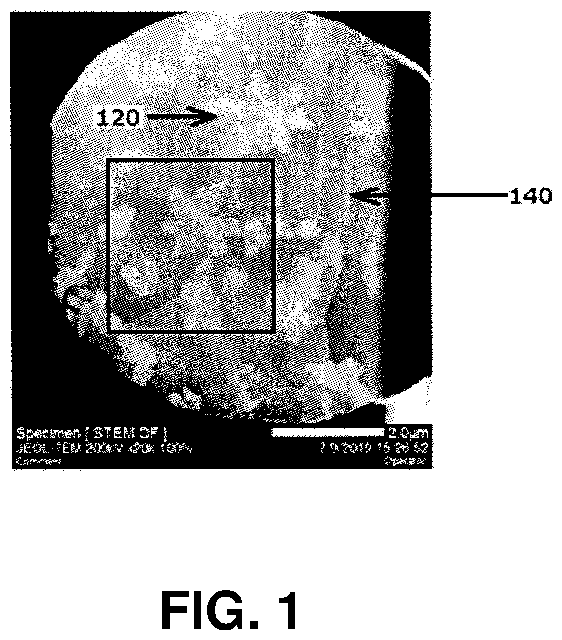
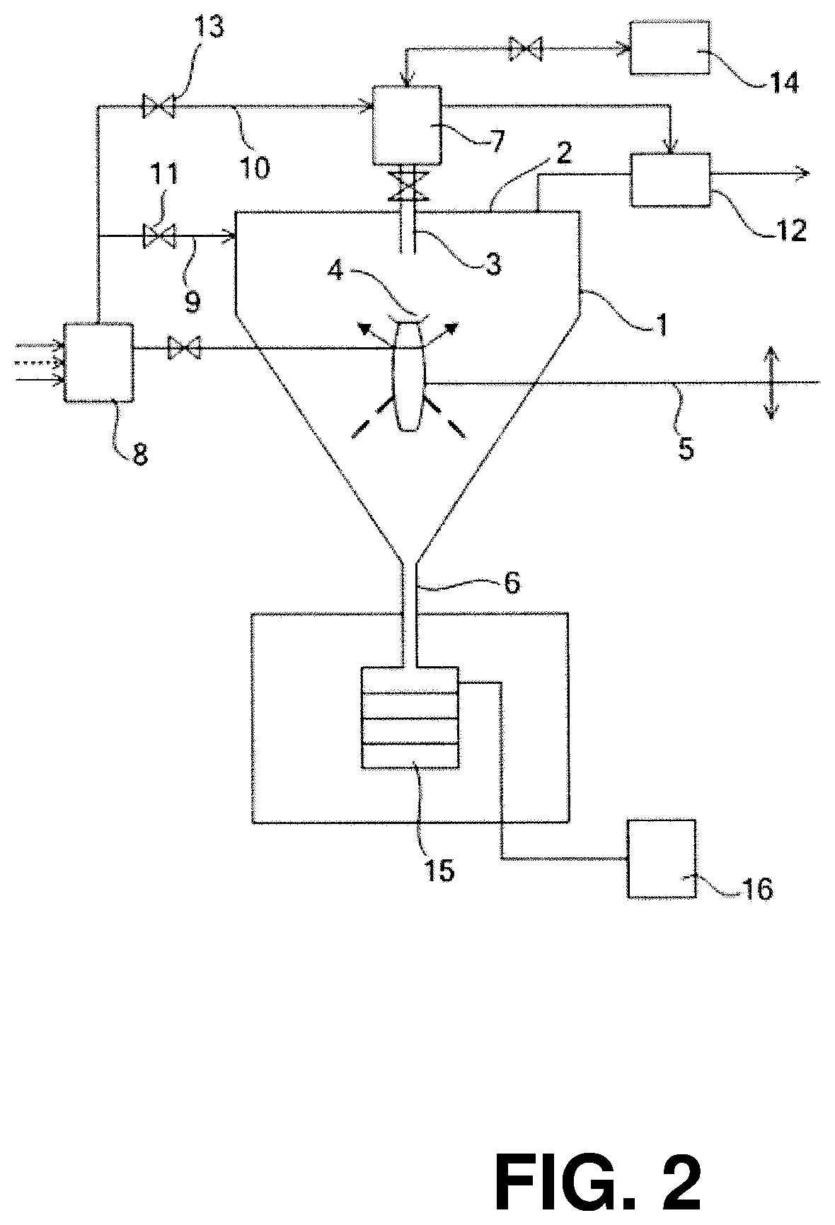
[0057]A metal particle having a diameter of approximately 3 to 13 μm was manufactured from a starting material composed of 8% by mass of Cu, 1% by mass of Ni, 0.001% by mass of Ge and the balance of Sn, with use of the manufacturing apparatus illustrated in FIG. 2.

[0058]Conditions below were employed for the process.

[0059]A melting crucible was placed in the electric furnace 7, into which the aforementioned starting material was placed and melted at 650° C., and while keeping the temperature, the molten metal was fed through the nozzle 3 onto the dish-like rotating disk 4.

[0060]The dish-like rotating disk 4 employed here was a dish-like disk with an inner diameter of 35 mm and a thickness of rotating plate of 5 to 3 mm, which was rotated at 80,000 to 100,000 rpm.

[0061]The granulation chamber 1 which can be evacuated down to around 9×10⁻² Pa was evacuated, to which nitrogen gas at 15 to 50° C. was fed and concurrently evacuated, to thereby adjust the inner pressure of the gr...

Example

Example 2

[0071]A metal particle 2 was manufactured in the same way as in Example 1, except by using a starting material composed of 8% by mass of Cu, 3% by mass of Ni, 0.1% by mass of Ge and the balance of Sn.

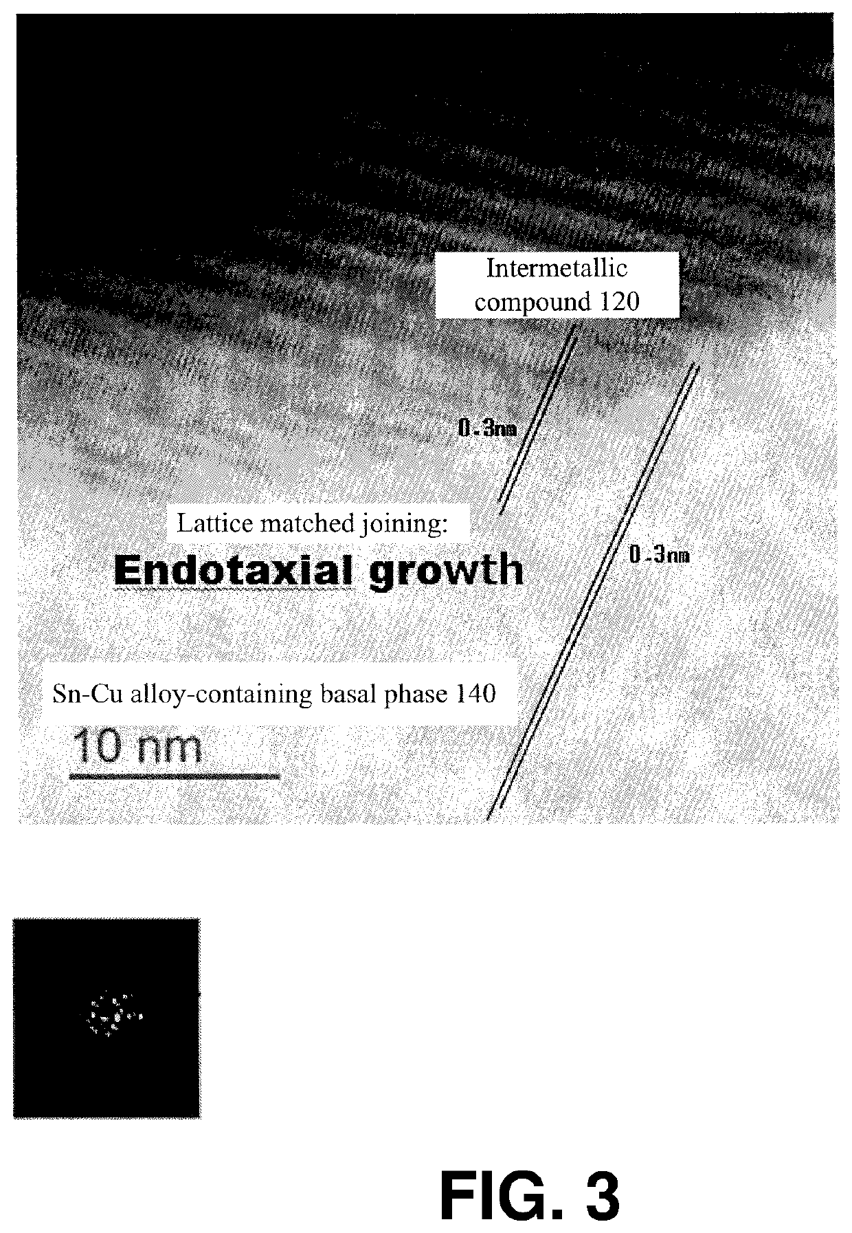
[0072]Next, 70% by mass of the metal particle 2, and 30% by mass of alloy powder composed of 90% by mass of Cu and 10% by mass of Ni were homogeneously mixed, and the mixture in a dry powder form was compressed to manufacture a sheet (50 μm thick). The sheet was then used for joining the copper substrate and the silicon device, and subjected to the high temperature storage test (HTS) at 260° C. Results indicated that shear strength elevated from approximately 60 MPa up to approximately 70 MPa, over a period ranging from the start of test until approximately 100 hours after, and remained plateau at approximately 60 MPa over a temporal range beyond 100 hours.

[0073]On the other hand, temperature cycle test (TCT) ranged from −40 to 200° C. yielded results indicating that the shear ...

Example

Comparative Example 1

[0074]As a comparative example, a prior SnAgCu-based joint material (powdery solder material with a particle size of 5 μm) was used as the joint material. The temperature cycle test (TCT) carried out in the same way as in Example 1 (−40 to 200° C.) revealed that the joint area caused decay before going through 100 cycles, which was far from achieving heat resistance and strength comparable to those of the metal particle of this invention.

[0075]The present inventors confirmed from our investigations that the prior SnAgCu-based joint material did not contain the intermetallic compound, instead allowing a single metal element to be dispersed therein. The present inventors also confirmed that the Sn—Cu alloy of the basal phase did not have a crystal structure of the high temperature phase.

[0076]FIG. 4 is an optical microphotograph of the surfaces of gold electrodes, observed after a sheet of a metal particle 1 (IMC) obtained in Example 1 and a sheet of an SnAgCu-bas...


PUM

PropertyMeasurementUnit
Temperatureaaaaaaaaaa

Abstract

A metal particle for joint material includes an intermetallic compound crystal that contains Sn, Cu, Ni and Ge, in a basal phase that contains Sn and an Sn—Cu alloy, the metal particle having a chemical composition represented by 0.7 to 15% by mass of Cu, 0.1 to 5% by mass of Ni, 0.001 to 0.1% by mass of Ge and the balance of Sn, the basal phase having a chemical composition represented by 95 to 99.9% by mass of Sn, 5% by mass or less of Cu and 0.1% by mass or less of an inevitable impurity, the intermetallic compound crystal residing in the basal phase so as to be included therein, the metal particle having a particle size of 1 μm to 50 μm, the metal particle containing an orthorhombic crystal structure, and at least parts of the basal phase and the intermetallic compound crystal forming an endotaxial joint.

Description

INCORPORATION BY REFERENCE[0001]This application is based on Japanese Patent Application No. 2020-42772, filed on Mar. 12, 2020, the content of which is incorporated hereinto by reference.BACKGROUND OF THE INVENTION1. Field of the Invention[0002]This invention relates to a metal particle.2. Description of the Related Art[0003]In an advancing situation of IoT (Internet of Things) with ever-growing needs for energy saving, power semiconductor that holds the key for the technology has been increasingly gaining its importance, while leaving many problems on effective use thereof to be solved. The power semiconductor, which handles high power ascribed to high voltage and large current and is used for ultra-high speed transmission, produces large amount of heat and becomes hot. Si power semiconductor, although having been suited to a required level of heat resistance of approximately 175° C. at present, are on the way to development towards a Si power semiconductor durable to higher tempe...

Claims


Application Information

Patent Timeline
IPC IPC(8): B23K35/26C22C13/00B22F1/00B22F9/08B22F1/05
CPCB23K35/262C22C13/00B22F2304/10B22F9/08B22F2301/30B22F1/0011B23K35/268B22F1/05B22F2999/00C22C2200/06C22C1/0483B22F2009/0844B22F9/082B22F7/064B22F2998/10B22F2201/02B22F3/02B22F5/006B22F2203/11B22F2203/13
Inventor SEKINE, SHIGENOBU
Owner NAPRA
Why Eureka
Try Eureka