Electrically rewritable non-volatile memory element and method of manufacturing the same

a non-volatile memory element, electric rewritability technology, applied in the direction of bulk negative resistance effect devices, electrical equipment, semiconductor devices, etc., can solve the problems of reducing the electrical power consumption of devices, dram is volatile memory that loses stored data, and the limit of device electrical power consumption, so as to reduce the contact area and suppress heat radiation to the bit line

Active Publication Date: 2009-09-01
MICRON TECH INC
View PDF2 Cites 21 Cited by
  • Summary
  • Abstract
  • Description
  • Claims
  • Application Information

AI Technical Summary

Benefits of technology

[0019]According to this aspect of the present invention, since the bit line is offset to a recording layer, it is possible to reduce a contact area between the recording layer and the upper electrode or a contact area between the upper electrode and the bit line even when an interlayer insulation film is not arranged between the upper electrode and the bit line. Therefore, it is possible to suppress heat radiation to the bit line while connecting the upper electrode and the bit line without using the through-hole.
[0020]In this case, the bit line is preferably offset to the recording layer so that a lower electrode and the bit line do not overlap. Thus, the distance between a phase change region in the recording layer and the bit line increases, thereby further suppressing the heat radiation to the bit line.
[0047]As described above, according to the present invention, it is possible to reduce a contact area between the recording layer and the upper electrode or a contact area between the upper electrode and the bit line without providing the interlayer insulation film between the upper electrode and the bit line. Thus, it is possible to suppress heat radiation to the bit line while connecting the upper electrode and the bit line without using a through-hole.

Problems solved by technology

DRAM is volatile memory that loses stored data if its power supply is turned off.
That makes DRAM unsuitable for the storage of programs and archival information.
Also, even when the power supply is turned on, the device has to periodically perform refresh operations in order to retain stored data, so there are limits as to how much device electrical power consumption can be reduced, while yet a further problem is the complexity of the controls run under the controller.
Semiconductor flash memory is high capacity and non-volatile, but requires high current for writing and erasing data, and write and erase times are slow.
These drawbacks make flash memory an unsuitable candidate for replacing DRAM in main memory applications.
There are other non-volatile memory devices, such as magnetoresistive random access memory (MRAM) and ferroelectric random access memory (FRAM), but, they cannot easily achieve the kind of storage capacities that are possible with DRAM.
The condition for forming the through-hole and the condition for embedding the conductive material increasingly become severe when the non-volatile memory element is further miniaturized.
Therefore, when the non-volatile memory element is further miniaturized, it becomes difficult to form the through-hole or to embed the conductive material.
Further, since a mask pattern for forming the through-hole in the interlayer insulation film is necessary, this becomes one of the factors that increase manufacturing costs.
As a result, heat radiation to the bit line increases, thereby greatly decreasing the heat efficiency.

Method used


Image

  • Electrically rewritable non-volatile memory element and method of manufacturing the same
  • Electrically rewritable non-volatile memory element and method of manufacturing the same
  • Electrically rewritable non-volatile memory element and method of manufacturing the same

Examples


second embodiment

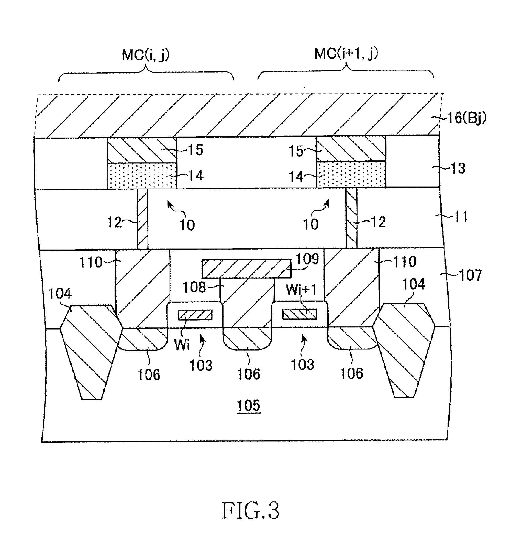
[0122]FIG. 17 is a schematic plan view of a structure of the non-volatile memory element 20 according to the present invention. FIG. 18 is a schematic cross section taken along a line E-E shown in FIG. 17. FIG. 19 is a schematic cross section taken along a line F-F shown in FIG. 17. FIG. 19 shows a structure of a memory cell that uses the non-volatile memory element 20 of this embodiment.

[0123]The non-volatile memory element 20 according to this embodiment is different from the non-volatile memory element 10 according to the first embodiment in that the inner portion of the through-hole 13a is formed with the recording layer 14 alone, and the upper electrode 15 is formed on the interlayer insulation film 13. The remaining respects of the non-volatile memory element 20 are the same as those of the non-volatile memory element 10 according to the first embodiment. Thus, like reference numerals denote like parts, and redundant explanations thereof will be omitted.

[0124]In this embodimen...

third embodiment

[0137]FIG. 24 is a schematic plan view of a structure of the non-volatile memory element 30 according to the present invention. FIG. 25 is a schematic cross section taken along a line G-G shown in FIG. 24. FIG. 26 is a schematic cross section taken along a line H-H shown in FIG. 24. FIG. 26 shows a structure of a memory cell that uses the non-volatile memory element 30 according to this embodiment.

[0138]The non-volatile memory element 30 according to this embodiment is different from the non-volatile memory element 10 according to the first embodiment in that side surfaces of the recording layer 14 and the upper electrode 15 are not covered with an interlayer insulation film but are covered with a sidewall insulation layer 31. The remaining respects of the non-volatile memory element 30 are the same as those of the non-volatile memory element 10 according to the first embodiment. Therefore, like reference numerals denote like parts, and redundant explanations thereof will be omitted...

first embodiment

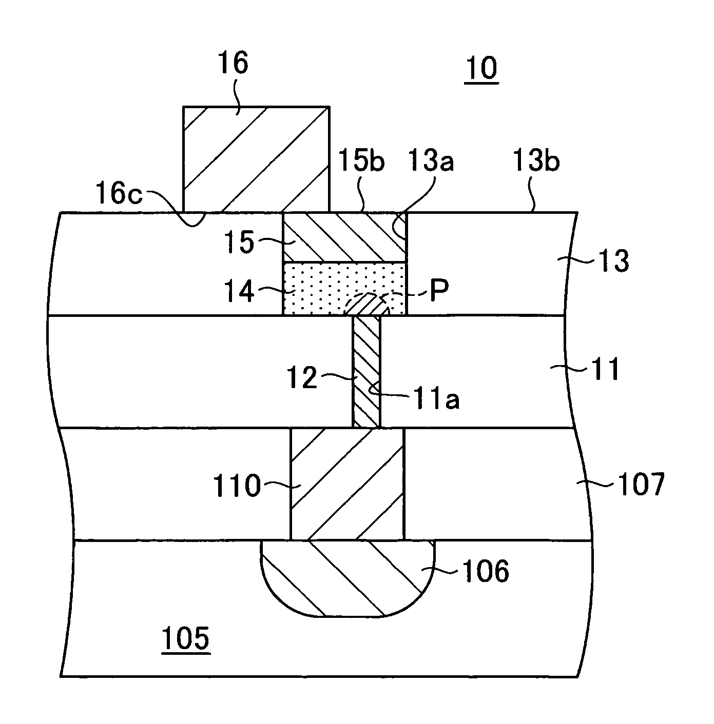
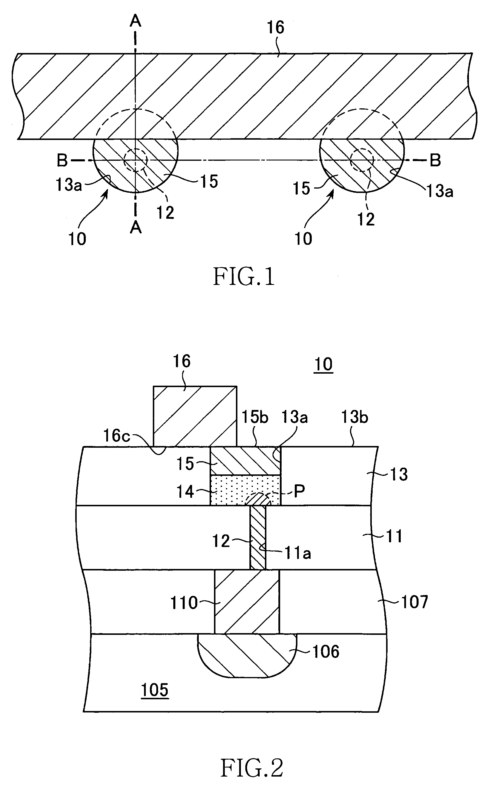
[0139]In this embodiment, the bit line 16 is formed so as to cover one portion of a boundary line between the upper electrode 15 and the sidewall insulation layer 31, as shown in FIG. 25. That is, the bit line 16 is formed so that the edge thereof traverses the upper electrode 15. Thus, one portion of the bottom surface 16c of the bit line 16 contacts one portion of the top surface 15b of the upper electrode 15. The remaining portion thereof contacts the sidewall insulation layer 31 and the interlayer insulation film 11. The remaining portion of the top surface 15b of the upper electrode 15 does not contact the bit line 16. Thus, in this embodiment, similarly to the first embodiment, the bit line 16 is arranged to be offset to the recording layer 14. As a result, a contact area between the bit line 16 and the upper electrode 15 is reduced, and the distance between the phase change region P and the bit line 16 can be increased.

[0140]A manufacturing method of the non-volatile memory e...


PUM


Abstract

A non-volatile memory element includes a lower electrode, an upper electrode, a recording layer arranged between the lower electrode and the upper electrode and containing a phase change material, and a bit line directly arranged on the upper electrode. The bit line is formed to be offset to the recording layer. With this arrangement, a contact area between the recording layer and the upper electrode and a contact area between the upper electrode and the bit line can be reduced without providing an interlayer insulation film between the upper electrode and the bit line. Thus, heat radiation to the bit line can be suppressed while the upper electrode and the bit line are connected without using a through-hole.

Description

TECHNICAL FIELD[0001]The present invention relates to an electrically rewritable non-volatile memory element and to a method of manufacturing the element. More specifically, the present invention relates to an electrically rewritable non-volatile memory element having a recording layer that includes phase change material, and to a method of manufacturing the element.BACKGROUND OF THE INVENTION[0002]Personal computers and servers and the like use a hierarchy of memory devices. There is lower-tier memory, which is inexpensive and provides high storage capacity, while memory higher up the hierarchy provides high-speed operation. The bottom tier generally consists of magnetic storage such as hard disks and magnetic tape. In addition to being non-volatile, magnetic storage is an inexpensive way of storing much larger quantities of information than solid-state devices such as semiconductor memory. However, semiconductor memory is much faster and can access stored data randomly, in contras...

Claims


Application Information

Patent Timeline
Patent Type & Authority Patents(United States)
IPC IPC(8): H01L47/00
CPCH01L27/2436H01L27/2463H01L45/06H01L45/1233H01L45/1683H01L45/143H01L45/144H01L45/1675H01L45/126H10B63/30H10B63/80H10N70/8413H10N70/8825H10N70/231H10N70/066H10N70/8828H10N70/063H10N70/826
Inventor ASANO, ISAMU
Owner MICRON TECH INC
Why Eureka
Try Eureka