Nonvolatile semiconductor memory having voltage adjusting circuit

a voltage adjustment circuit and semiconductor technology, applied in static storage, digital storage, instruments, etc., can solve the problems of reducing the operation margin and reducing the yield of semiconductor memory to a large extent. , to achieve the effect of increasing the operation margin, increasing the yield, and increasing the yield of nonvolatile semiconductor memory

Active Publication Date: 2009-09-08
LONGITUDE FLASH MEMORY SOLUTIONS LTD
View PDF3 Cites 7 Cited by
  • Summary
  • Abstract
  • Description
  • Claims
  • Application Information

AI Technical Summary

Benefits of technology

[0009]An object of the present invention is to increase operation margins of a nonvolatile semiconductor memory and thereby increase its yield.
[0010]According to a first aspect of the invention, nonvolatile evaluation memory cells are programmed in advance to be set to a plurality of different values, respectively. An internal voltage generating circuit generates an internal voltage to be used in an internal circuit. The internal voltage generating circuit can change the value of the internal voltage according to an adjusting signal. To make the internal voltage close to an expected value, a voltage adjusting circuit outputs, in a read operation on the evaluation memory cells, the adjusting signal in accordance with cell currents which flow through the respective evaluation memory cells. In general, with variations in manufacturing conditions of a semiconductor memory, the characteristics of constituent elements, such as transistors, of the semiconductor memory also vary. As a result, the internal voltage generated by the internal voltage generating circuit varies and cell currents flowing through the evaluation memory cells in a read operation also vary. Therefore, a variation in the interval voltage generated by the internal voltage generating circuit can be detected as variations in the cell currents. This makes it possible to automatically set the internal voltage shifted due to variations in manufacturing conditions to the expected value, by using an adjusting signal. Since the internal circuit operates on a correct internal voltage, operation margins can be increased. As a result, the yield of the nonvolatile semiconductor memory can be increased.
[0011]This makes it possible to automatically set the timing of the control signal shifted due to variations in manufacturing conditions to the expected timing by using an adjusting signal. Since the internal circuit operates with a control signal having correct timing, operation margins can be increased. As a result, the yield of the nonvolatile semiconductor memory can be increased.

Problems solved by technology

In particular, where the boost circuit operates only in accessing memory cells and a boosted voltage is generated by supplying a pulse signal to one end of the capacitor, it is difficult to finely adjust the boosted voltage through monitoring it.
This may lower the yield of the semiconductor memory to a large extent.
This means a problem that the boosted voltage cannot be adjusted chip by chip.
As a result, it is impossible to, generate an optimum boosted voltage for each chip.
In other words, the effect of increasing the operation margins is not sufficient.

Method used


Image

  • Nonvolatile semiconductor memory having voltage adjusting circuit
  • Nonvolatile semiconductor memory having voltage adjusting circuit
  • Nonvolatile semiconductor memory having voltage adjusting circuit

Examples


first embodiment

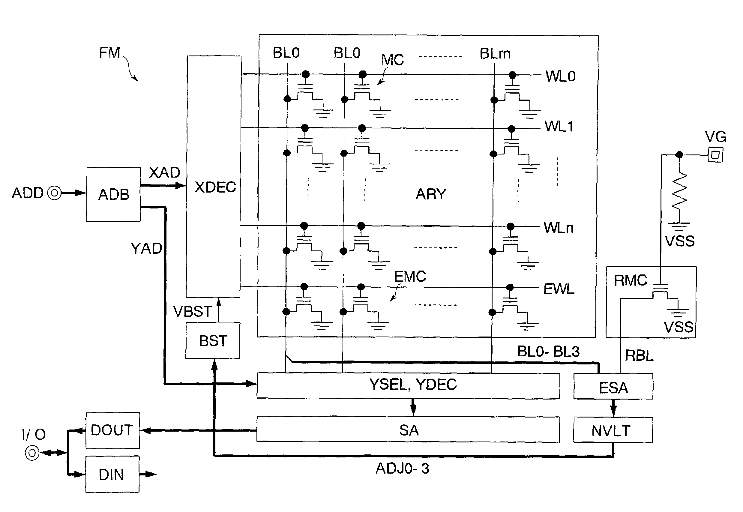
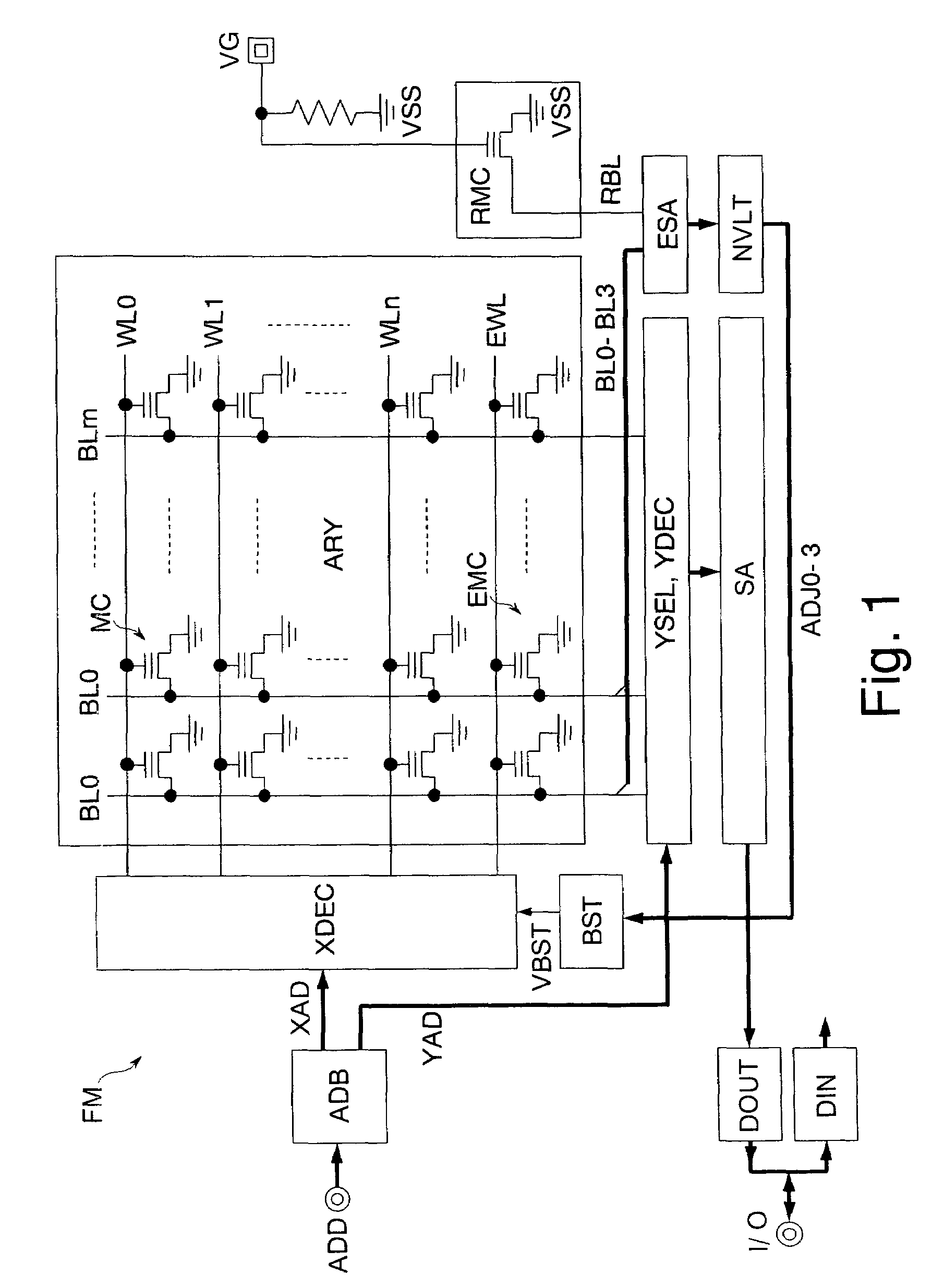
[0022]FIG. 1 shows a nonvolatile semiconductor memory according to the invention. This nonvolatile semiconductor memory is a NOR flash memory FM which has electrically rewritable nonvolatile memory cells and is manufactured on a silicon substrate by a CMOS process.

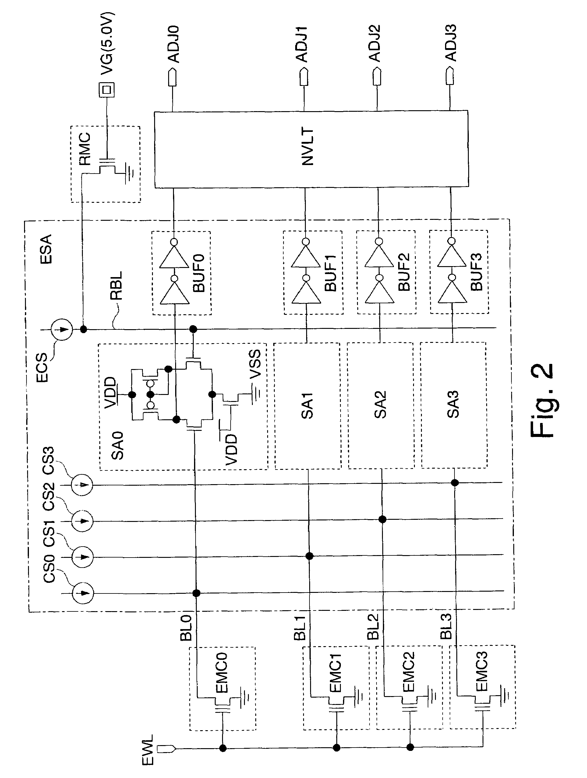
[0023]The flash memory FM has an address buffer ADB, a data input buffer DIN, a data output buffer DOUT, a boost circuit BST (internal voltage generating circuit), a word decoder XDEC, a memory cell array ARY, a column decoder YDEC, a column selector YSEL, a sense amplifier SA, an evaluation sense amplifier ESA (voltage adjusting circuit), a nonvolatile latch NVLT (nonvolatile memory circuit), and a reference memory cell RMC.

[0024]The address buffer ADB receives an address signal AD via an address terminal AD and outputs the received address AD as a row address signal XAD and a column address signal YAD. The row address signal XAD consists of higher bits of the address signal AD. The row address signal XAD is used for a se...

second embodiment

[0081]The second embodiment is such that the timing of generation of a column timing signal CLT, a sense amplifier timing signal SAT, and a data output timing signal DOT is changed in accordance with a high-level voltage of the evaluation word line EWL. However, only the timing of generation of a word timing signal WLT to be used for setting output timing of a word line signal WL (i.e., activation timing and deactivation timing of a word line WL) may be changed in accordance with the high-level signal of the evaluation word line EWL without changing the timing of generation of a column timing signal CLT, a sense amplifier timing signal SAT, and a data output timing signal DOT.

[0082]More specifically, if a high-level voltage of the evaluation word line EWL is low, the timing of generation of a word timing signal WLT is advanced. If a high-level voltage of the evaluation word line EWL is high, the timing of generation of a word timing signal WLT is delayed. This makes it possible to m...


PUM


Abstract

Nonvolatile evaluation memory cells are programmed to be a plurality of different values in advance, respectively. An internal voltage generating circuit can change the value of an internal voltage according to adjusting signals. To make the internal voltage close to its expected value, a voltage adjusting circuit outputs adjusting signals in accordance with cell currents that flow through the evaluation memory cells, respectively, in a read operation on the evaluation memory cells. As a result, the interval voltage that is shifted from its expected value due to variations in manufacturing conditions can automatically be set to the expected value by using the adjusting signals. Since an internal circuit operates on a correct internal voltage, operation margins can be increased. The yield of a nonvolatile semiconductor memory can thus be increased.

Description

CROSS REFERENCE TO RELATED APPLICATION[0001]This application is based upon and claims the benefit of priority from Japanese Patent Application No. 2005-348912, filed on Dec. 2, 2005, the entire contents of which are incorporated herein by reference.BACKGROUND OF THE INVENTION[0002]1. Field of the Invention[0003]The present invention relates to a nonvolatile semiconductor memory having nonvolatile memory cells and word lines connected to the memory cells.[0004]2. Description of the Related Art[0005]Due to the miniaturization of semiconductor device structures, the insulator film of transistors has been thinning. To prevent reduction of the reliability of transistors, the power supply voltage supplied to a nonvolatile semiconductor memory such as a flash memory has been decreasing. Where an internal voltage (e.g., a high-level voltage of the word lines) used for accessing memory cells is higher than a power supply voltage, it is necessary to form, in the nonvolatile semiconductor memo...

Claims


Application Information

Patent Timeline
Patent Type & Authority Patents(United States)
IPC IPC(8): G11C16/06
CPCG11C16/26
Inventor MAWATARI, HIROSHIHIBINO, NORITOEMI, NAOTO
Owner LONGITUDE FLASH MEMORY SOLUTIONS LTD
Why Eureka
Try Eureka