Method of making thin film transistor liquid crystal display

a technology of thin film transistor and liquid crystal display, which is applied in the direction of photomechanical equipment, instruments, originals for photomechanical treatment, etc., can solve the problems of high process cost and inability to simplify the process, and achieve the effect of lowering the manufacturing cos

Inactive Publication Date: 2009-09-15
WINTEK CORP
View PDF1 Cites 0 Cited by
  • Summary
  • Abstract
  • Description
  • Claims
  • Application Information

AI Technical Summary

Benefits of technology

[0007]The primary objective of the present invention is to provide a method of making a thin film transistor array substrate, which the number of photomasks used in the process is reduced to lower the manufacture cost.
[0008]The secondary objective of the present invention is to provide a method of making a thin film transistor liquid crystal display, which increases the aperture ratio.

Problems solved by technology

However, the more photomasks used in the process take the higher cost for the process and cannot simplify the process.

Method used


Image

  • Method of making thin film transistor liquid crystal display
  • Method of making thin film transistor liquid crystal display
  • Method of making thin film transistor liquid crystal display

Examples


Embodiment Construction

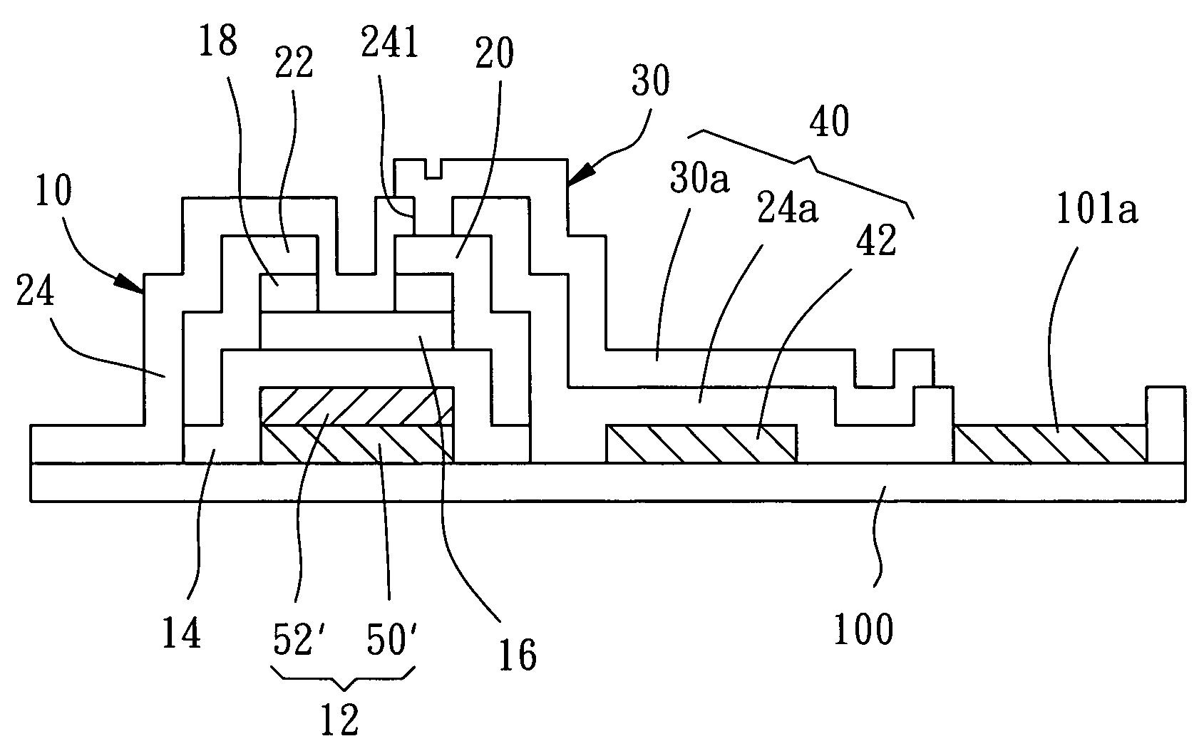
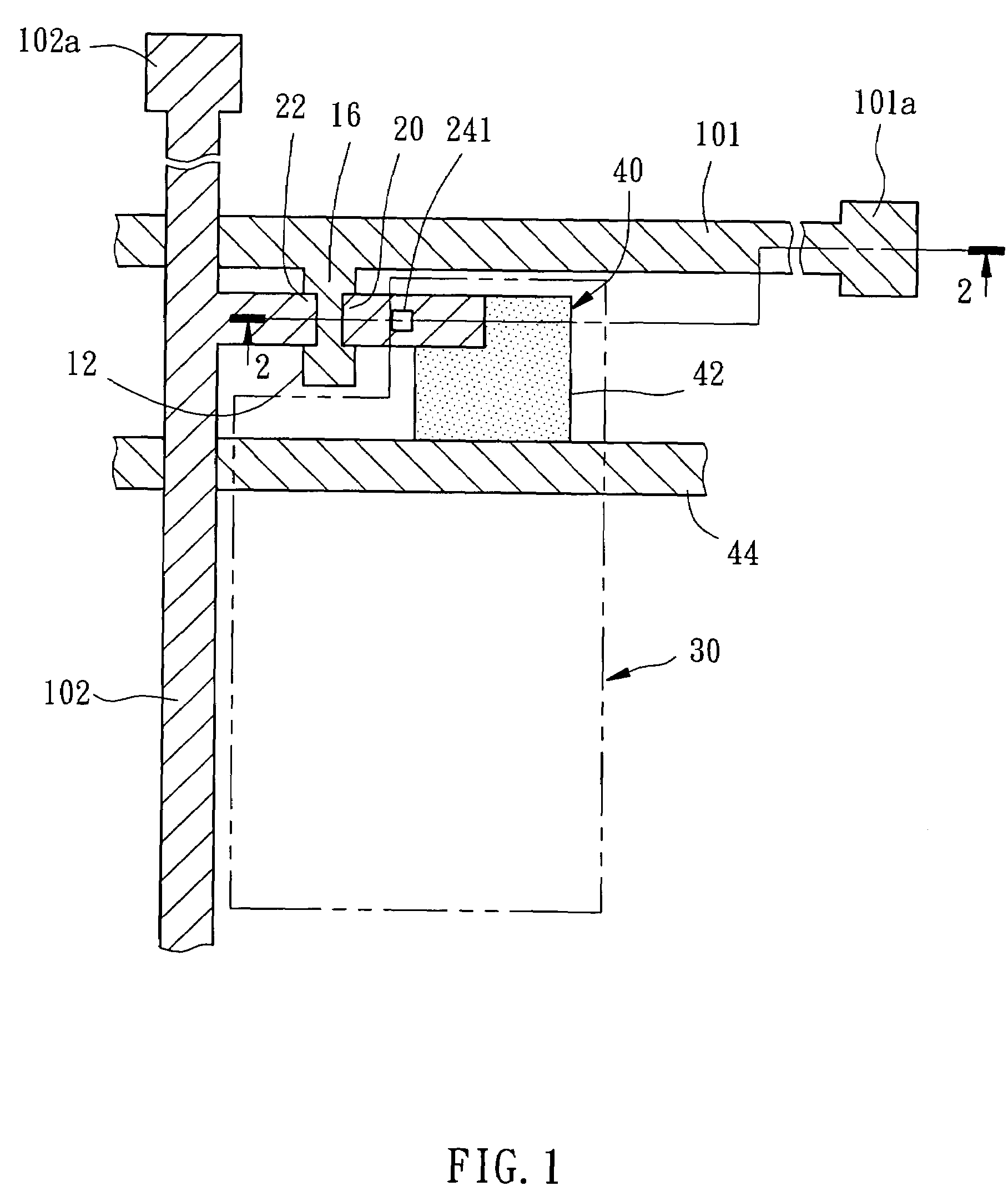
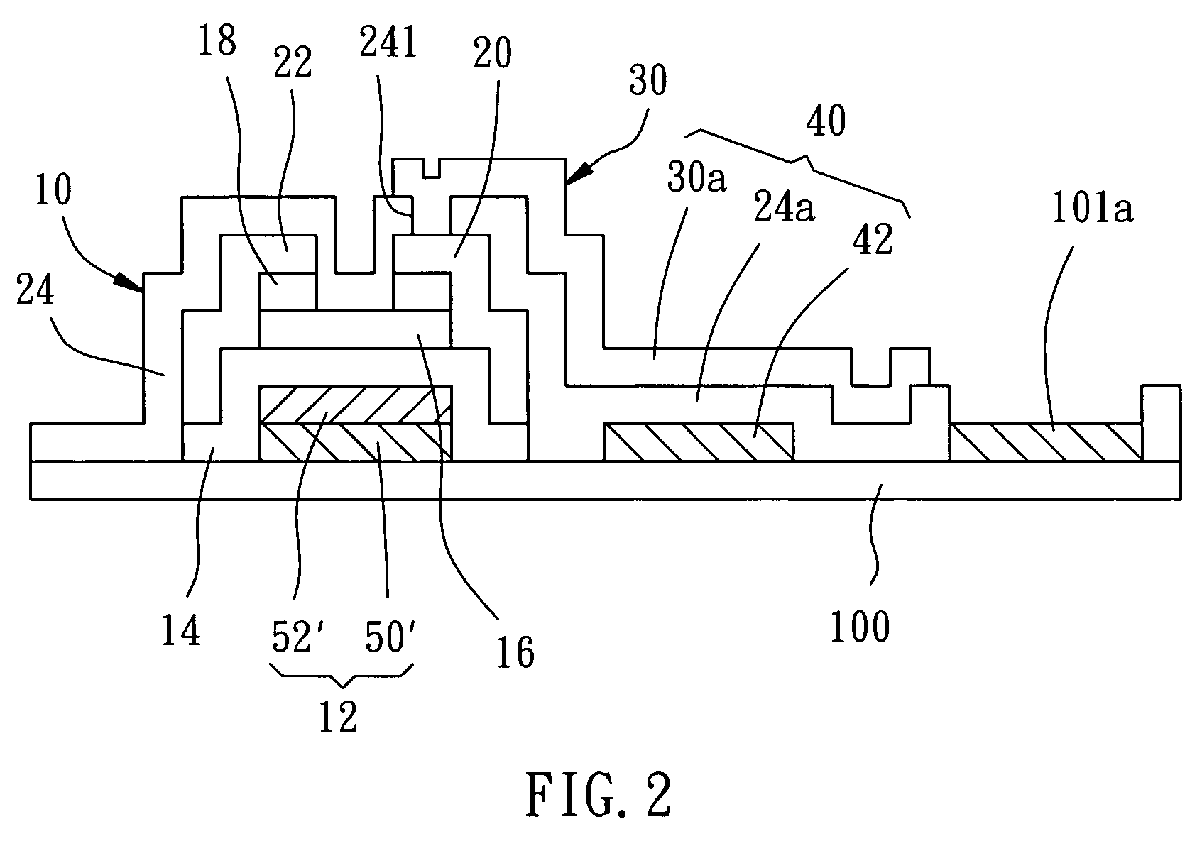
[0023]As shown in FIGS. 1 and 2, a thin film transistor array substrate of the preferred embodiment of the present invention includes a transparent substrate 100 with a plurality of scan lines 101 and data lines 102 thereon. The scan lines 101 and the data lines 102 are perpendicular and cross to each other to form a plurality of subpixels therebetween. The scan lines 101 have a first terminal portion 101a at an end thereof, and the data lines 102 have a second terminal portion 102a at an end thereof. The first terminal portion 101a and the second terminal portion 102a are electrically connected to a driving circuit. Each of the subpixels have an amorphous silicon thin film transistor (a-Si TFT) 10, a pixel electrode 30 and a storage capacitor (Cst) 40. These components are described hereunder:

[0024]The a-Si TFT 10 is an island-like structure with layers (from a bottom to a top) including a gate 12, a gate insulating layer 14, a channel layer 16, an ohmic contact layer 18, a source ...


PUM

PropertyMeasurementUnit
transparent conductiveaaaaaaaaaa
transparentaaaaaaaaaa
semi-transparentaaaaaaaaaa

Abstract

A thin film transistor liquid array substrate includes forming a plurality of amorphous silicon thin film transistors and storage capacities on a transparent substrate, wherein the amorphous silicon thin film transistors and the storage capacities are arranged in an array pattern. The storage capacitor has a top electrode and a bottom electrode, which are made of transparent conductive material to increase aperture ratio. A method of making the amorphous silicon thin film transistors and the storage capacities includes four photomask processes and a back exposure technique. Because the present invention only uses four photomask processes, the number of photomasks used in the process of the present invention is less than the conventional method, and the cost of fabrication is lower also.

Description

BACKGROUND OF THE INVENTION[0001]1. Field of the Invention[0002]The present invention relates generally to a thin film transistor liquid crystal display (TFT-LCD), and more particularly to a method of making a thin film transistor liquid crystal display fabricated through four photomask processes.[0003]2. Description of the Related Art[0004]A conventional thin film transistor liquid crystal display primarily includes a thin film transistor (TFT) array substrate, a color filter and a liquid crystal layer, wherein the TFT array substrate includes a transparent substrate with a plurality of scan lines and data lines. These scan lines and data lines are perpendicular to define a plurality of subpixels. In each subpixel, there is a thin film transistor, a storage capacitor and a pixel electrode. The thin film transistor is used to be a switch member of the liquid crystal display, which includes a gate, a gate insulating layer, a channel layer, an ohmic contact layer, a source / drain, a pa...

Claims


Application Information

Patent Timeline
Patent Type & Authority Patents(United States)
IPC IPC(8): H01L21/00G01F7/00
CPCH01L27/1214G03F7/0007H01L27/1255H01L27/1288
Inventor CHANG, CHIN-SHANWANG, WEN-CHUNWU, FA-CHEN
Owner WINTEK CORP
Why Eureka
Try Eureka