Controlling system for gate formation of semiconductor devices

a gate formation and control system technology, applied in the direction of individual semiconductor device testing, semiconductor/solid-state device testing/measurement, instruments, etc., can solve the problems of equipment generally not providing immediate feedback to the photolithography process, adversely affecting the performance of the finished semiconductor device, and resist loss

Inactive Publication Date: 2009-09-15
TAIWAN SEMICON MFG CO LTD
View PDF10 Cites 26 Cited by
  • Summary
  • Abstract
  • Description
  • Claims
  • Application Information

AI Technical Summary

Problems solved by technology

Deviations of a feature's critical dimension and profile from design dimensions may adversely affect the performance of the finished semiconductor device.
Furthermore, the measurement of a feature's critical dimension and profile may indicate processing problems, such as stepper defocusing or photo-resist loss due to over-exposure.
Although equipment is available for measuring device gate critical dimensions and profiles, such equipment generally does not provide immediate feedback to the photolithography process to reduce variations, and the results of conventional inspections are not typically used to adjust subsequent etch processing.
Furthermore, due to process variations, gate critical dimension and profile may be affected by factors unknown to designers, making it difficult to have a universal setting for process control.

Method used


Image

  • Controlling system for gate formation of semiconductor devices
  • Controlling system for gate formation of semiconductor devices
  • Controlling system for gate formation of semiconductor devices

Examples


Embodiment Construction

[0019]The making and using of the presently preferred embodiments are discussed in detail below. It should be appreciated, however, that the present invention provides many applicable inventive concepts that can be embodied in a wide variety of specific contexts. The specific embodiments discussed are merely illustrative of specific ways to make and use the invention, and do not limit the scope of the invention.

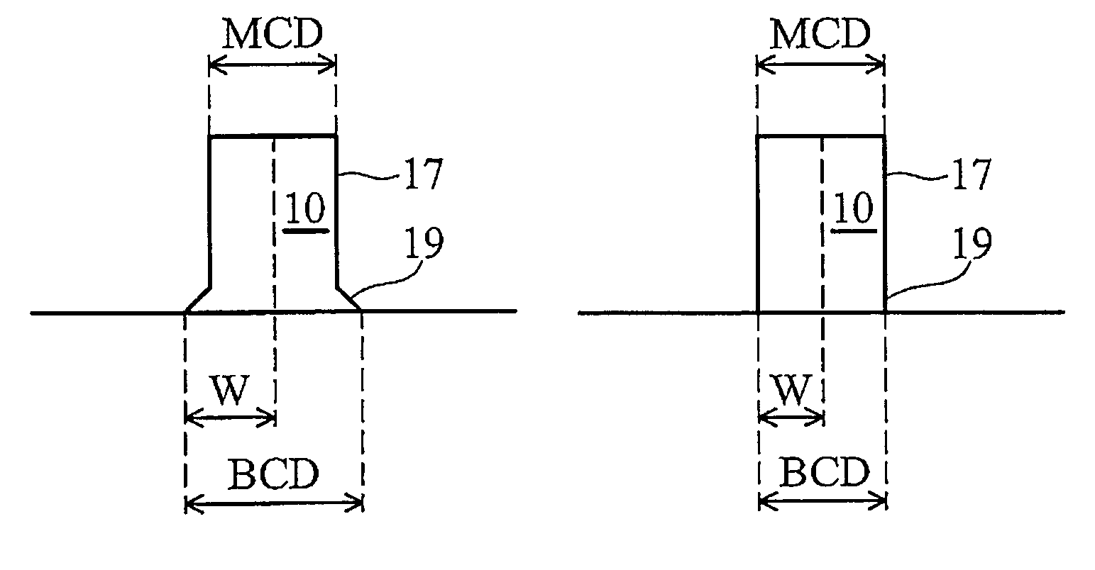
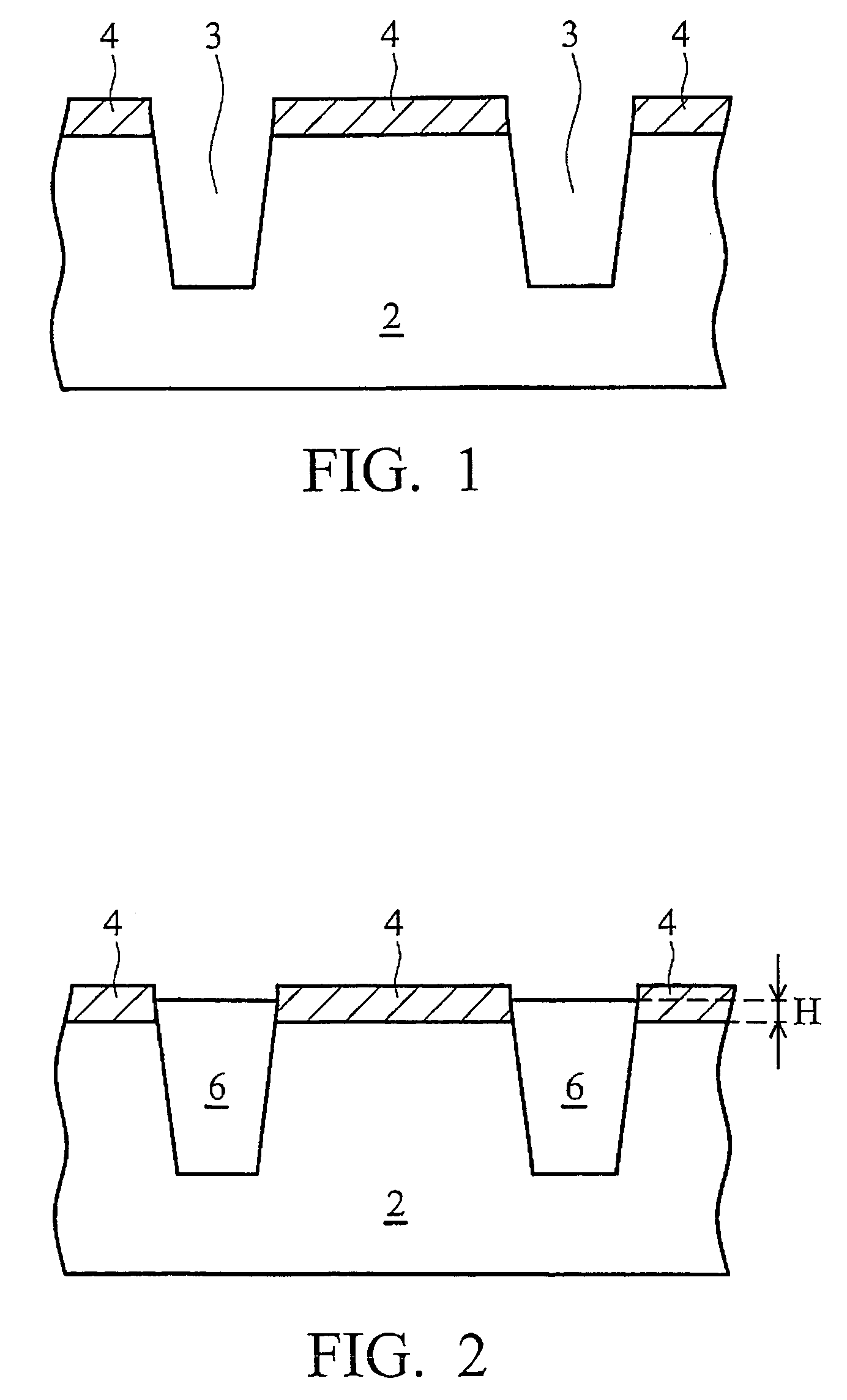
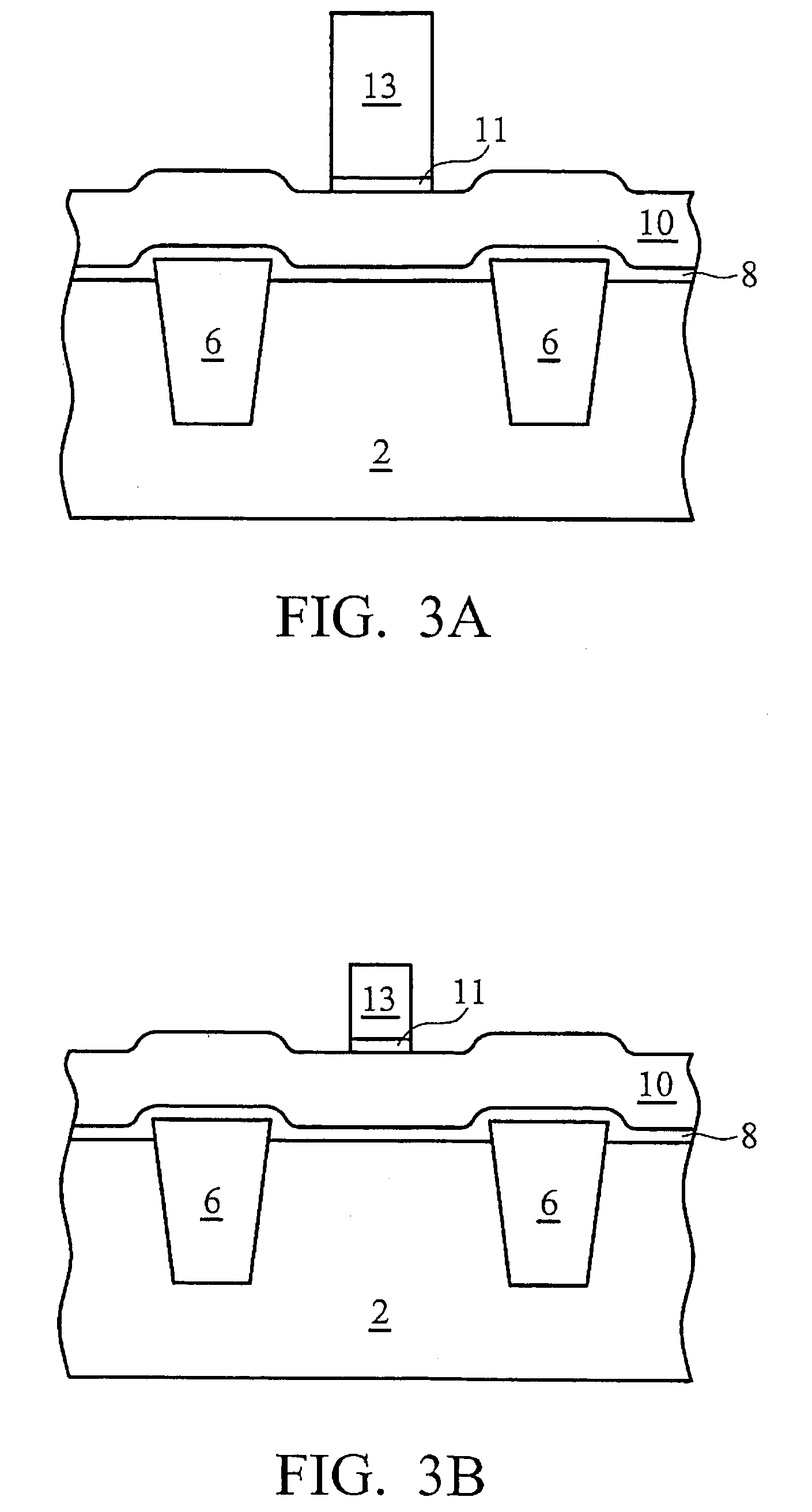
[0020]FIGS. 1 through 4 illustrate a typical MOS device and its formation, including the formation of STIs 6. A mask layer 4 is formed on an active region 2. In the preferred embodiment, mask layer 4 is formed of silicon nitride using low-pressure chemical vapor deposition (LPCVD). In other embodiments, mask layer 4 is formed by thermal nitridation of silicon, plasma enhanced chemical vapor deposition (PECVD) or plasma anodic nitridation using nitrogen-hydrogen. Trenches 3 are anisotropically etched through mask layer 4, or silicon nitride 4, into the active region 2. The tre...


PUM


Abstract

A method of controlling gate formation of semiconductor devices includes determining the correlation between the step heights of isolation structures and the over-etching time by measuring step heights of isolation structures, determining an over-etching time based on the step heights, and etching gates using the over-etching time. The method may include an after-etching-inspection to measure the gate profile and fine-tune the gate formation control. Within-wafer uniformity can also be improved by measuring the step height uniformity on a wafer and adjusting gate formation processes.

Description

TECHNICAL FIELD[0001]This invention relates generally to manufacturing processes of semiconductor devices, and more particularly to gate formation control of semiconductor devices.BACKGROUND[0002]Current demands for high density and performance associated with ultra large-scale integrated circuits require sub-micron features, increased transistor and circuit speeds, and improved reliability. Such demands require formation of device features with high precision and uniformity, which in turn necessitates careful process monitoring, including frequent and detailed inspections of the devices while they are still in the form of semiconductor wafers.[0003]As design rules shrink and process windows (i.e., the margins for error in processing) become smaller, inspection and measurement of surface features' critical dimensions (CD), defined as the smallest width of a line or the smallest space between two lines permitted in the fabrication of the device, as well as their cross-sectional shape...

Claims


Application Information

Patent Timeline
Patent Type & Authority Patents(United States)
IPC IPC(8): H01L21/00
CPCH01L22/12H01L22/26H01L21/28123H01L21/76224H01L2924/0002H01L2924/00
Inventor TSO, CHIA-TSUNGLAI, JIUN-HONGWU, MEI-JENHSU, LI TESU, PIN CHIACHEN, PO-ZEN
Owner TAIWAN SEMICON MFG CO LTD
Why Eureka
Try Eureka