
Photoelectric conversion device manufacturing method, semiconductor device manufacturing method, photoelectric conversion device, and image sensing system

a technology semiconductor device, which is applied in the field of photoelectric conversion device manufacturing method, semiconductor device manufacturing method, photoelectric conversion device, image sensing system, etc., can solve the problems of reducing the sensitivity of pd 1001/b>, difficult to accurately form semiconductor regions having different thicknesses in a predetermined region of a semiconductor substrate, and difficult to implant impurity ions to a predetermined depth, etc., to suppress crosstalk and improve the sensitivity of photoelectric conversion uni

Inactive Publication Date: 2009-09-22
CANON KK
View PDF21 Cites 27 Cited by
  • Summary
  • Abstract
  • Description
  • Claims
  • Application Information

AI Technical Summary

Benefits of technology

The present invention aims to improve the sensitivity and accuracy of photoelectric conversion units in a semiconductor device. Specifically, the invention provides a method for manufacturing a photoelectric conversion device with improved sensitivity and reduced crosstalk between adjacent photoelectric conversion units. Additionally, the invention allows for the formation of semiconductor regions with different thicknesses at a predetermined depth or more in a semiconductor substrate. The invention also includes a method for manufacturing a semiconductor substrate with a photoelectric conversion device and an image sensing system.

Problems solved by technology

This may lead to a decrease in the sensitivity of the PD 1001.
In a method of manufacturing a general semiconductor device including a photoelectric conversion device, it is difficult to accurately form semiconductor regions having different thicknesses in a predetermined region of a semiconductor substrate.
It is therefore difficult to implant impurity ions to a predetermined depth or more in the semiconductor substrate.
This may degrade the accuracy in the lateral direction when forming impurity regions having different concentrations in the semiconductor substrate.
In particular, crystal defects in the latter process have a particularly large influence on a photoelectric conversion device.
This may cause white defects fatal in an image obtained by the photoelectric conversion device.
This may make it difficult to design a desired profile and result in residual defects.

Method used


Image

  • Photoelectric conversion device manufacturing method, semiconductor device manufacturing method, photoelectric conversion device, and image sensing system
  • Photoelectric conversion device manufacturing method, semiconductor device manufacturing method, photoelectric conversion device, and image sensing system
  • Photoelectric conversion device manufacturing method, semiconductor device manufacturing method, photoelectric conversion device, and image sensing system

Examples


Embodiment Construction

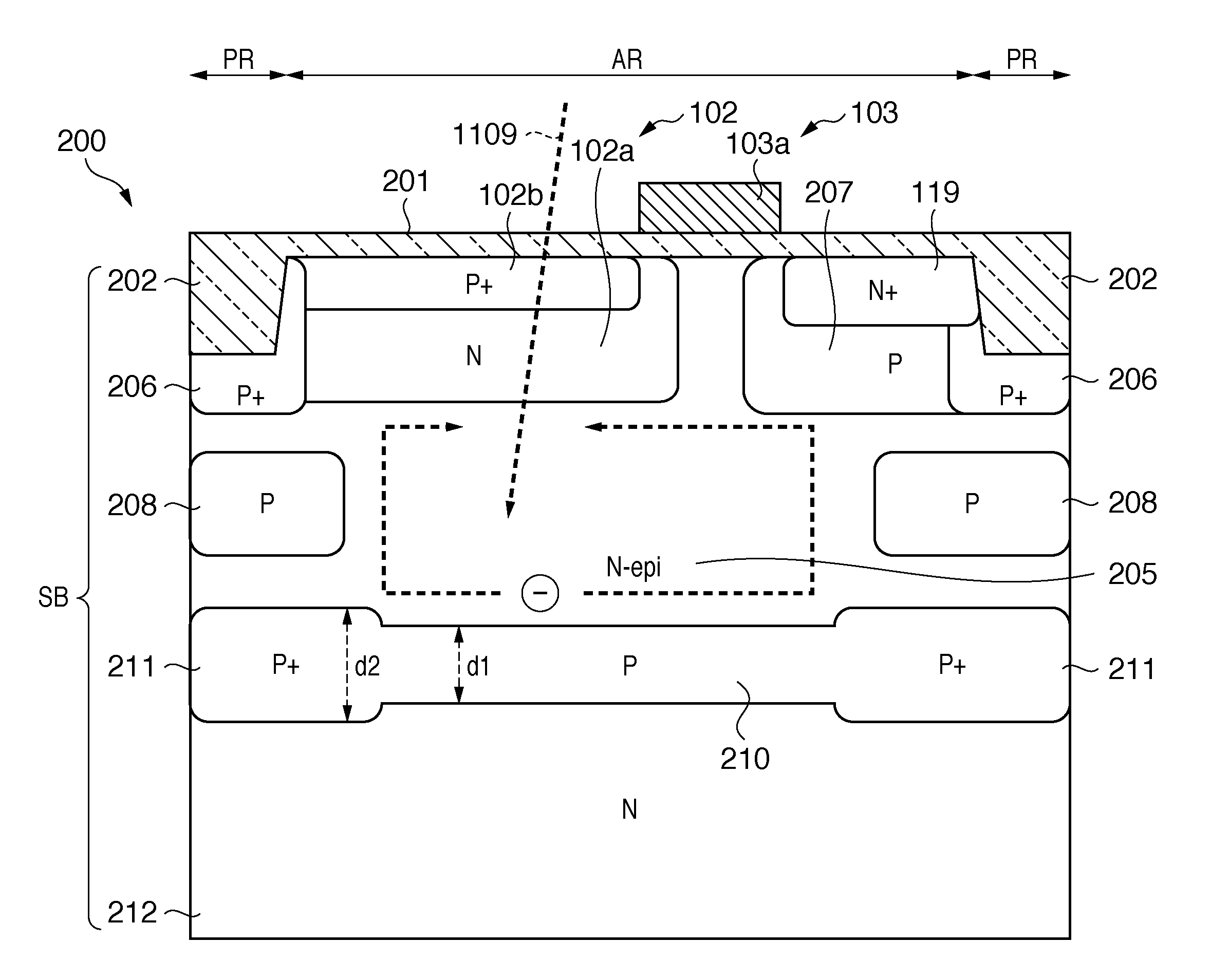
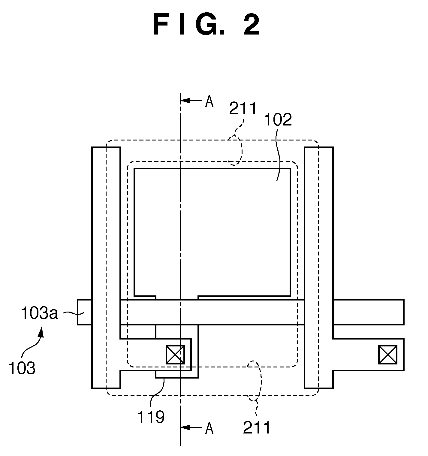
[0044]The embodiments of the present invention will now be described with reference to the accompanying drawings. Each embodiment of the present invention will be explained in association with a photoelectric conversion device. However, the embodiments are also applicable to any other semiconductor devices. The other semiconductor devices include a memory device such as a DRAM and a logic device such as a microcomputer.

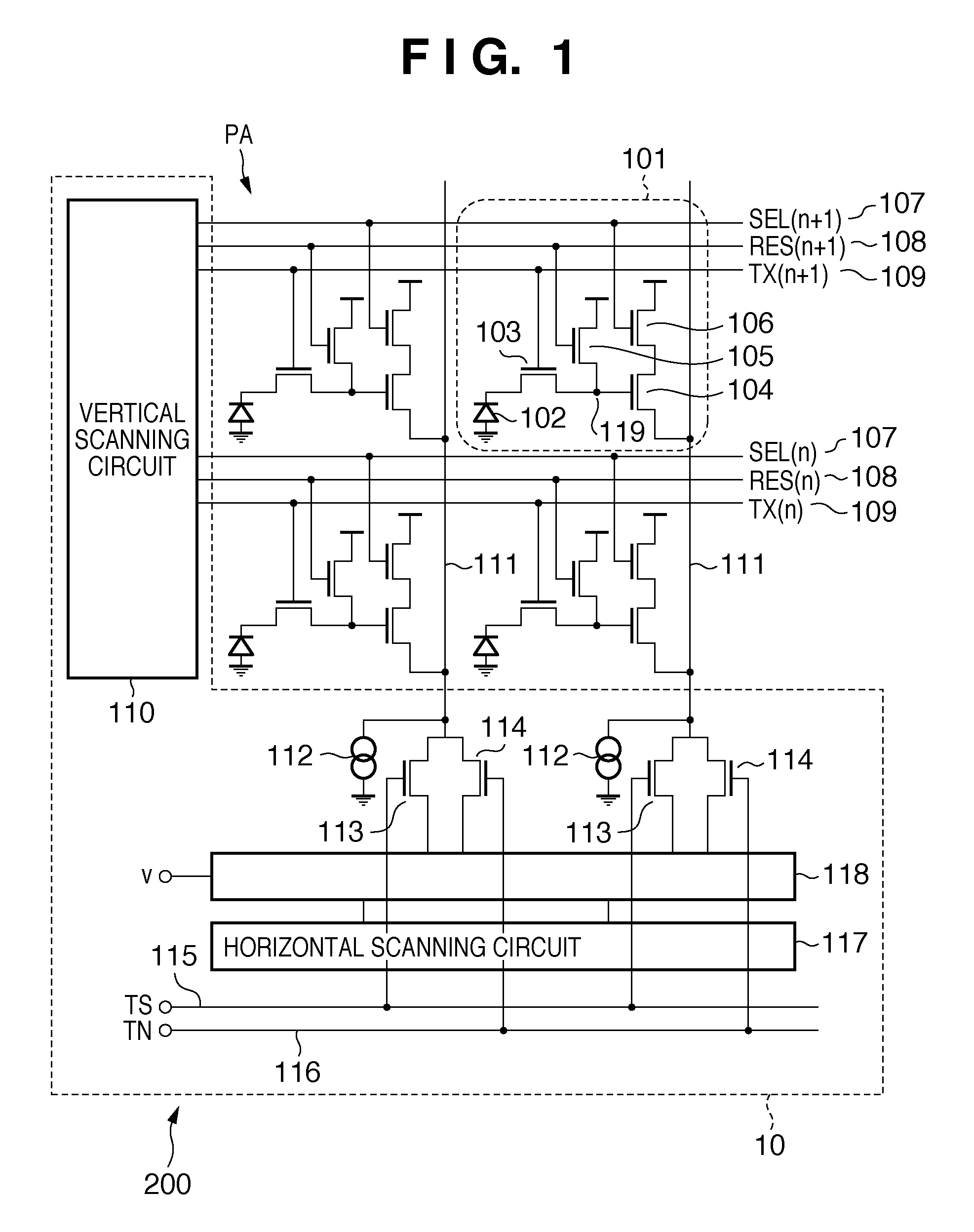
[0045]A photoelectric conversion device 200 according to the first embodiment of the present invention will be described with reference to FIG. 1. FIG. 1 is a block diagram of the photoelectric conversion device 200 according to the first embodiment of the present invention.

[0046]The photoelectric conversion device 200 includes a pixel array PA and a control portion 10.

[0047]In the pixel array PA, a plurality of pixels 101 are arrayed in the row and column directions. FIG. 1 illustrates the plurality of pixels 101 arrayed in 2 rows×2 columns. Each pixel 101 includes a...


PUM


Abstract

A photoelectric conversion device manufacturing method comprises: a first implantation step of implanting impurity ions of a first conductivity type into an underlying substrate via a region of the oxide film exposed by an opening, thereby forming a first semiconductor region having a first thickness in the element region; an the oxidation step of oxidizing the region of the oxide film exposed by the opening, thereby thickening the exposed region; an the exposure step of exposing a region of the oxide film which is not exposed by the opening; a the second implantation step of, after the exposure step, implanting the impurity ions of the first conductivity type into the underlying substrate via a region unthickened in the oxidation step, thereby forming a second semiconductor region having a second thickness larger than the first thickness in the element isolation region; and an the element formation step.

Description

BACKGROUND OF THE INVENTION[0001]1. Field of the Invention[0002]The present invention relates to a photoelectric conversion device manufacturing method, semiconductor device manufacturing method, photoelectric conversion device, and image sensing system.[0003]2. Description of the Related Art[0004]A photoelectric conversion device is recently used in a two-dimensional image input apparatus represented by a digital still camera and a video camcorder or a one-dimensional image reading apparatus represented by a facsimile apparatus and a scanner. The demand for photoelectric conversion devices is rapidly growing.[0005]A photoelectric conversion device uses, for example, a CCD (Charge Coupled Device) or a MOS sensor. CMOS sensors have been in practical use as a typical MOS sensor.[0006]A CMOS sensor includes a pixel array and a control portion.[0007]In the pixel array, a plurality of pixels are arrayed in the row and column directions. Each pixel has a circuit arrangement shown in FIG. ...

Claims


Application Information

Patent Timeline
Patent Type & Authority Patents(United States)
IPC IPC(8): H01L27/00H01L27/146H04N25/00
CPCH01L27/14603H01L27/14689H01L27/1463
Inventor TAMURA, SEIICHIITANO, TETSUYA
Owner CANON KK
Learn More