Partial FinFET memory cell

a memory cell and finfet technology, applied in the field of memory cells, can solve the problems of affecting the drive current of pull-down nmos devices, affecting the performance of pmos and nmos devices, and affecting so as to achieve more balanced pmos and nmos performance, and improve the performance of memory cells

Active Publication Date: 2009-09-22
TAIWAN SEMICON MFG CO LTD
View PDF7 Cites 25 Cited by
  • Summary
  • Abstract
  • Description
  • Claims
  • Application Information

AI Technical Summary

Benefits of technology

[0011]The embodiments of the present invention have more balanced PMOS and NMOS performance, and thus the performance of memory cells is improved.

Problems solved by technology

Continued scaling of MOSFETs results in severe degradation of carrier mobility, however, which in turn adversely affects the device drive current.
The drive currents of pull-down NMOS devices, however, are relatively difficult to improve, and thus have smaller drive currents.
The unbalanced performance of PMOS and NMOS devices causes a writing problem.
Consequently, when a “0” is written into the memory cell, it takes a long period of time to write the state “0.” Additionally, write margins of the SRAM cells are degraded due to the high drive currents of PMOS devices.
A low write margin results in an increased possibility of erroneous writing.
Such a solution, however, contradicts to the requirement of scaling integrated circuits.
Therefore, increasing gate width of NMOS devices in memories is not a preferred method.

Method used


Image

  • Partial FinFET memory cell
  • Partial FinFET memory cell
  • Partial FinFET memory cell

Examples


Embodiment Construction

[0020]The making and using of the presently preferred embodiments are discussed in detail below. It should be appreciated, however, that the present invention provides many applicable inventive concepts that can be embodied in a wide variety of specific contexts. The specific embodiments discussed are merely illustrative of specific ways to make and use the invention, and do not limit the scope of the invention.

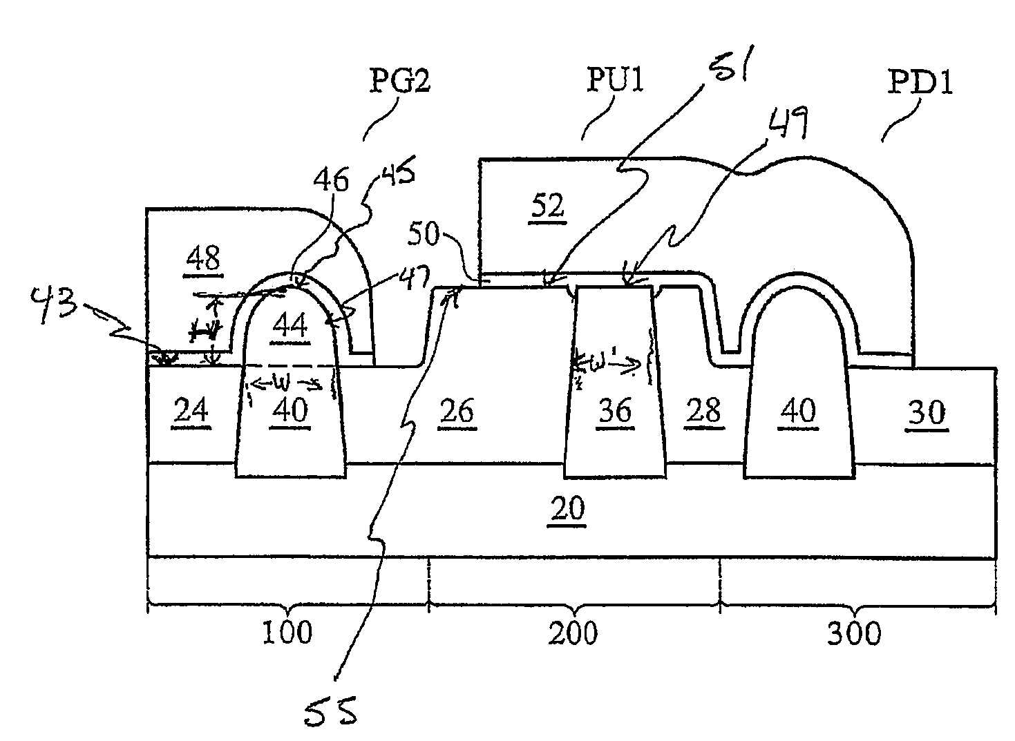
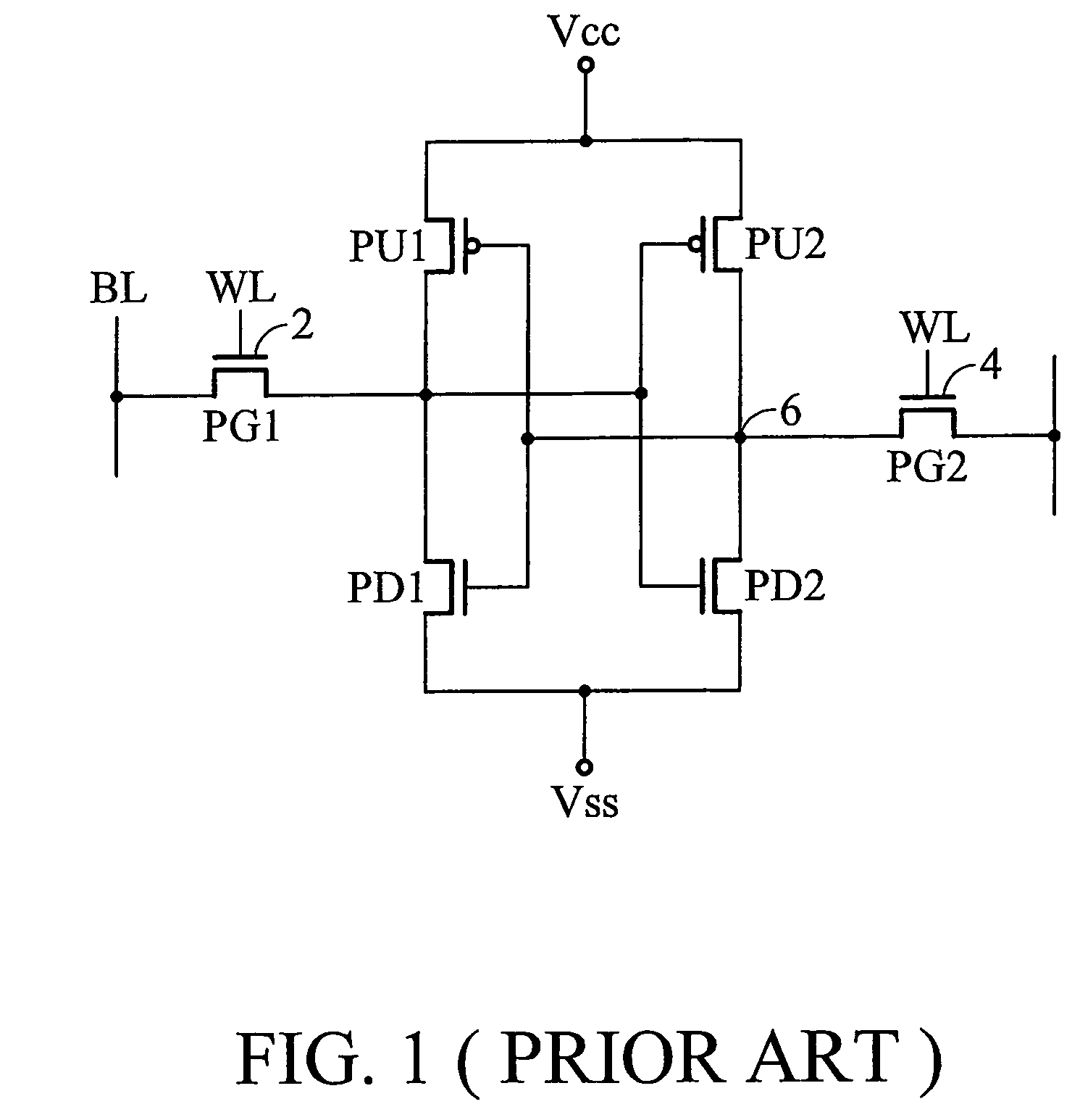
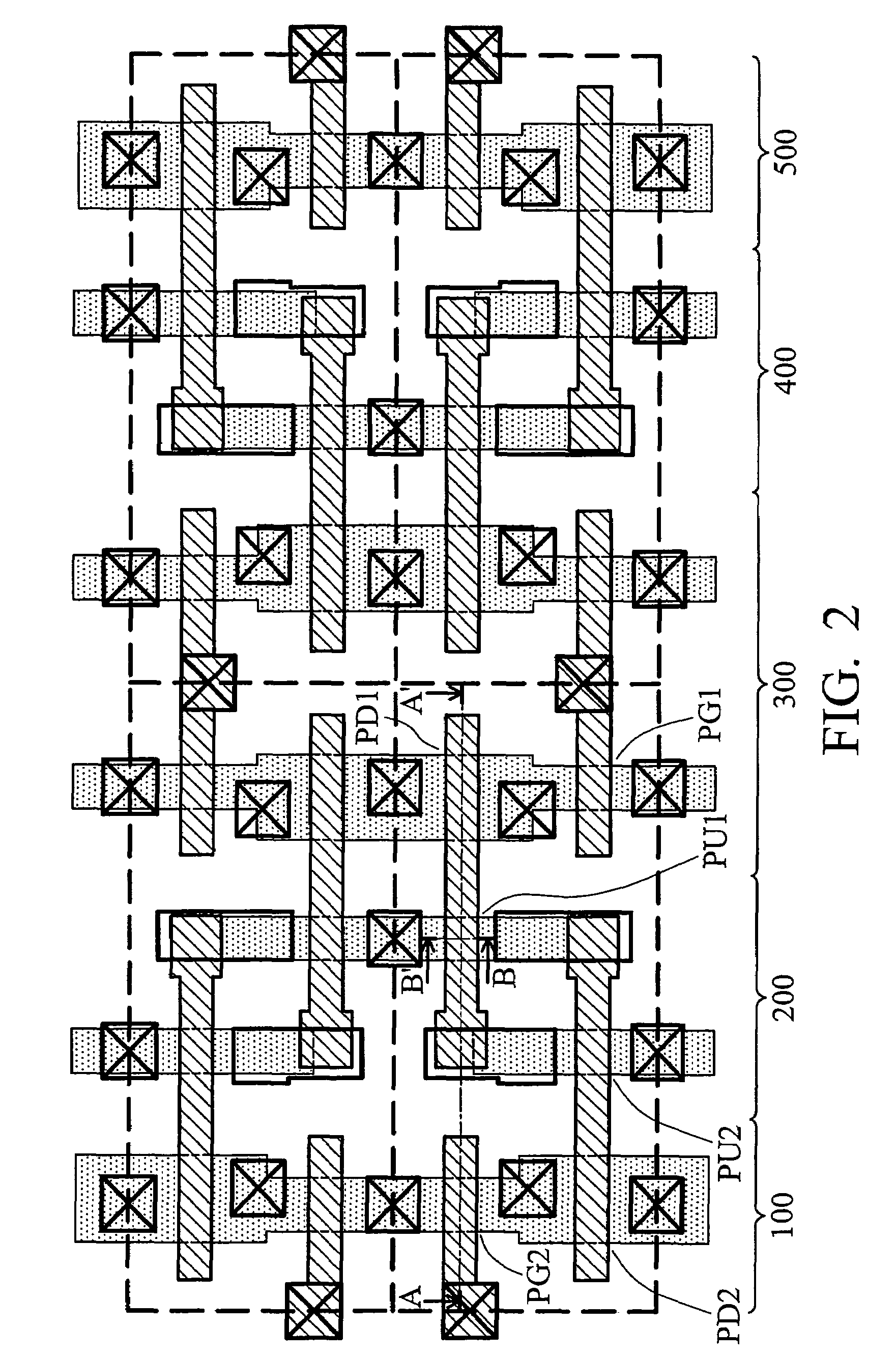
[0021]FIG. 2 illustrates an exemplary layout of an embodiment of the present invention. Four six-transistor (6T) unit memory cells are formed, each being inside a region defined by dotted lines. The layout illustrates p-well regions 100, 300 and 500, which are for forming n-type metal-oxide-semiconductor (MOS) devices, and n-well regions 200 and 400, which are for forming p-type MOS devices. For simplicity, in the subsequent illustrated drawings, only the unit memory cell at left bottom corner of FIG. 2 is discussed.

[0022]In the illustrated exemplary layout, each unit memory ...


PUM


Abstract

A semiconductor structure includes a semiconductor substrate, a planar PMOS device at a surface of the semiconductor substrate, and an NMOS device at the surface of the semiconductor substrate, wherein the NMOS device is a Fin field effect transistor (FinFET).

Description

[0001]This application claims the benefit of U.S. Provisional Application No. 60 / 849,047, filed on Oct. 2, 2006, entitled A Partial FinFET Memory Cell, which application is hereby incorporated herein by reference.TECHNICAL FIELD[0002]This invention relates generally to semiconductor devices, and more particularly to memory cells, and even more particularly to the fabrication of integrated circuits comprising static random access memory cells.BACKGROUND[0003]Scaling of semiconductor devices (e.g., a metal-oxide semiconductor field-effect transistor) has enabled continued improvement in speed, performance, density, and cost per unit function of integrated circuits over the past few decades. Continued scaling of MOSFETs results in severe degradation of carrier mobility, however, which in turn adversely affects the device drive current. To further enhance the performance of MOS devices, carrier mobility enhancement becomes a key element in developing next-generation technologies. Among ...

Claims


Application Information

Patent Timeline
Patent Type & Authority Patents(United States)
IPC IPC(8): H01L27/092
CPCH01L27/11H01L27/1104H01L27/1108H01L29/7854H01L29/785H10B10/125H10B10/00H10B10/12
Inventor LIAW, JHON-JHY
Owner TAIWAN SEMICON MFG CO LTD
Why Eureka
Try Eureka