Electrical circuit, apparatus and method for the demodulation of an intensity-modulated signal

an intensity-modulated signal and electric circuit technology, applied in the field of sensing and measurement techniques, can solve the problems of incompatibility with the small pixel size, power consumption, complex signal multiplication, etc., and achieve the effects of low electric power consumption, simple driving, and compact siz

Active Publication Date: 2009-09-29
CSEM CENT SUISSE DELECTRONIQUE & DE MICROTECHNIQUE SA RECH & DEV
View PDF3 Cites 11 Cited by
  • Summary
  • Abstract
  • Description
  • Claims
  • Application Information

AI Technical Summary

Benefits of technology

[0009]It is an object of the invention to provide an electric circuit with which the spatially and temporally resolved amplitude and phase of a temporally modulated signal can be detected for the purpose of demodulation, but which do not suffer from the disadvantages of the prior art. The circuits should be integrable in dense one- or two-dimensional arrays due to their compact size, low electric power consumption, simplicity of driving, independent signal pre-processing capabilities and robustness of operation regarding fabrication tolerances of semiconductor processes. It is a further object of the invention to provide a one- or two-dimensional array sensor and an apparatus for the spatially and temporally resolved demodulation of a modulated signal. It is still another object of the invention to provide a method for the detection of a modulated signal. These and other objects are achieved by the electric circuit, the array sensor, the apparatus and the method defined in the independent claims. Advantageous embodiments are defined in the dependent claims.

Problems solved by technology

While several electronic circuits and digital signal processing algorithms exist that can provide this demodulation function for a single measurement spot, none of these solutions allow the integration into dense, massively parallel and reliably operating arrays of demodulation photosensors.
Its disadvantage is the need for large RC-constants for frequencies below 10 kHz, which are not compatible with the small pixel size and the new CMOS processes.
But signal multiplication is complex and power consuming compared to the power available in each pixel (typically a few μW) and therefore not suited for massive parallel integration in a pixel field.
Digital signal demodulation algorithms are normally too complex to be implemented into a pixel (more than 50 transistors).
But all of them imply multiplication and are therefore not applicable in a power efficient pixel structure.

Method used


Image

  • Electrical circuit, apparatus and method for the demodulation of an intensity-modulated signal
  • Electrical circuit, apparatus and method for the demodulation of an intensity-modulated signal
  • Electrical circuit, apparatus and method for the demodulation of an intensity-modulated signal

Examples


Embodiment Construction

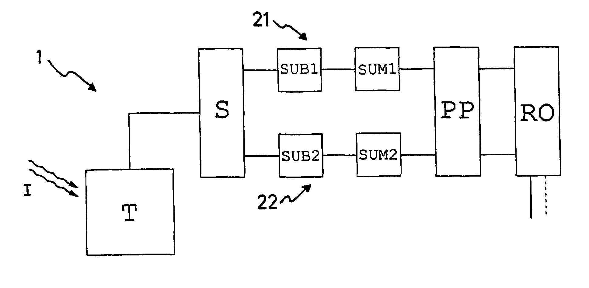
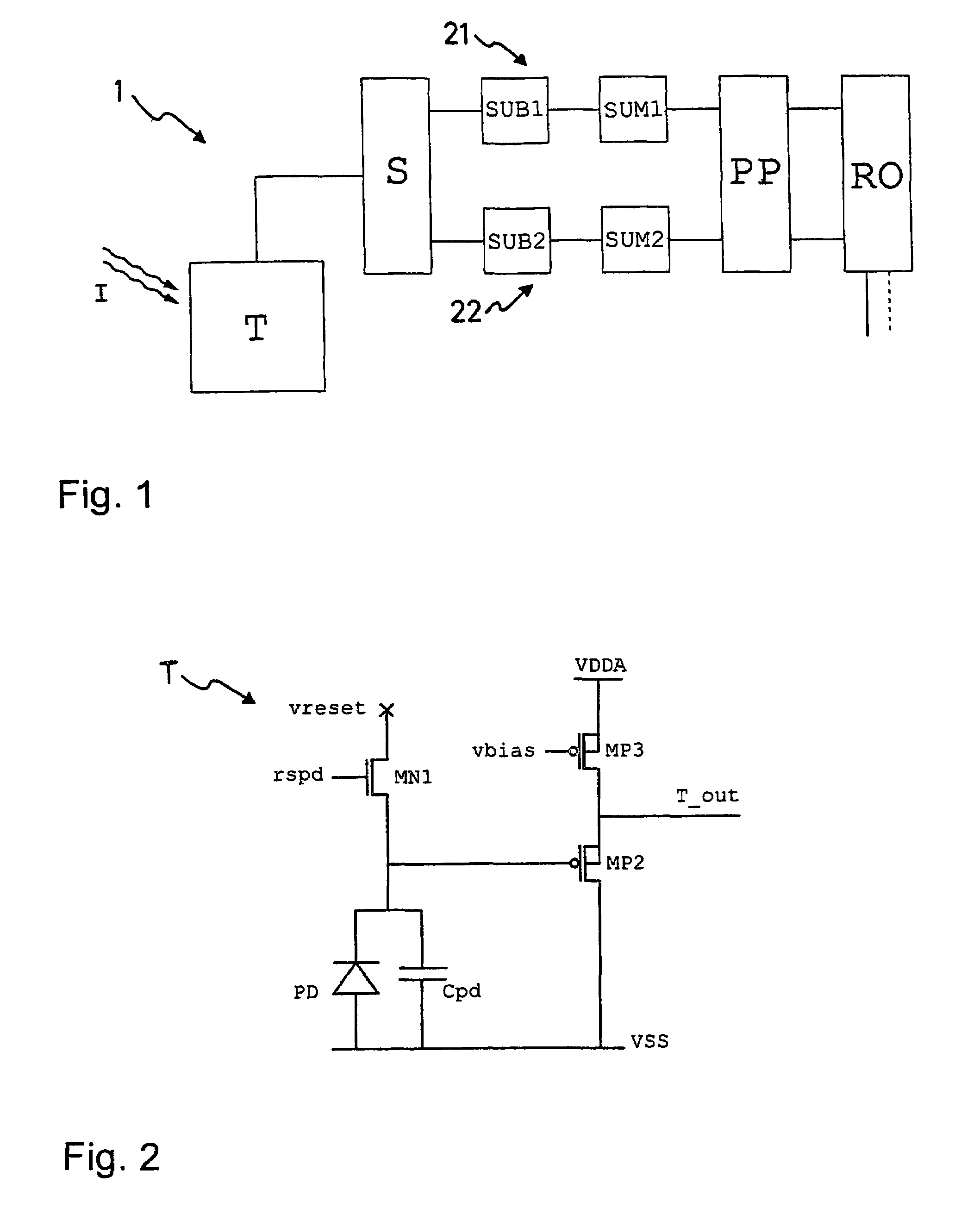
[0031]FIG. 1 shows a block diagram of an electrical circuit 1 or a demodulation pixel according to the invention. The electrical circuit 1 comprises a transduction stage T, a sampling or sample and hold stage S, two subtraction stages SUB1 and SUB2, two summation stages SUM1 and SUM2, a signal preprocessing stage PP and a readout stage RO. After the sampling stage S, the signal path is split into two channels 21, 22: a first channel 21 includes the first subtraction stage SUB1 and behind it the first summation stage SUM1, and a second channel 22 includes the second subtraction stage SUB2 and behind it the second summation stage SUM2.

[0032]An input signal I, which is preferably an optical radiation field, is sensed in the transduction stage T and transduced to an electrical signal of any kind (e.g., charge, voltage or current as described for example in U.S. Pat. No. 6,469,489 by S. Bourquin and P. Seitz). The transduction stage T may have an approximate or exact offset compensation,...


PUM


Abstract

A modulated optical radiation field (I) whose modulation amplitude and temporal phase depend on the local position can be detected with a plurality of pixels 1. Each pixel 1 consists of a transducing stage (T) that converts incoming light (I) into a proportional electric signal, a sampling stage (S), two subtraction / summation stages (SUB1, SUM1; SUB2, SUM2), and an output stage. Each pixel can be addressed individually. The optical radiation field (I) is locally sensed and sampled at a frequency that is four times the wavefield's modulation frequency. The subtraction / summation stages (SUB1, SUM1; SUB2, SUM2) accumulate differences of two samples per modulation period, separated by half the period, during several averaging periods; the two stages are time shifted with respect to each other by a quarter period. The resulting two output signals are employed for the determination of the local envelope amplitude and the temporal phase. These pixels 1 can be realized with circuits that consume very little electric power require small areas, enabling the realization of large numbers of pixels in linear or two-dimensional array sensors.

Description

[0001]This application is a §371 national phase filing of PCT / CH2004 / 000122 filed Mar. 3, 2004, and claims priority to a European application No. 03405164.9 filed Mar. 10, 2003.FIELD OF THE INVENTION[0002]This invention generally relates to all sensing and measurement techniques that rely on temporally modulated signals, preferably optical radiation fields, whose local variation of amplitude and phase must be measured as a function of time. More particularly, it relates to all of these sensing and measurement techniques that require dense one- or two-dimensional arrays of such amplitude- and phase-sensitive demodulation pixels. These techniques include optical coherence tomography (OCT), time-of-flight (TOF) range imaging and multiple wave interferometry.BACKGROUND OF THE INVENTION[0003]Many optical sensing and measurement techniques are known that are based on temporally modulated optical radiation fields whose local amplitude and phase vary as a function of time. These techniques ...

Claims


Application Information

Patent Timeline
Patent Type & Authority Patents(United States)
IPC IPC(8): H01J40/14G01J4/00H03D7/02
CPCH03D7/02H03D3/00H03D3/08
Inventor BEER, STEPHANSEITZ, PETER
Owner CSEM CENT SUISSE DELECTRONIQUE & DE MICROTECHNIQUE SA RECH & DEV
Why Eureka
Try Eureka