Digital interface decode receiver apparatus

a receiver and digital interface technology, applied in the field of digital interface decode receivers, can solve problems such as circuit destruction, increase in consumption power, or thermal runaway, and achieve the effect of preventing abnormalities

Active Publication Date: 2009-09-29
PANASONIC CORP
View PDF35 Cites 28 Cited by
  • Summary
  • Abstract
  • Description
  • Claims
  • Application Information

AI Technical Summary

Benefits of technology

[0011]It is an object of the present invention to provide a digital interface decode receiver in which abnormalities are prevented even when receiving a digital signal having a format other than decodable ones.

Problems solved by technology

This may cause abnormalities such as thermal runaway, increases in consumption power, or circuit destruction.

Method used


Image

  • Digital interface decode receiver apparatus
  • Digital interface decode receiver apparatus
  • Digital interface decode receiver apparatus

Examples


first embodiment

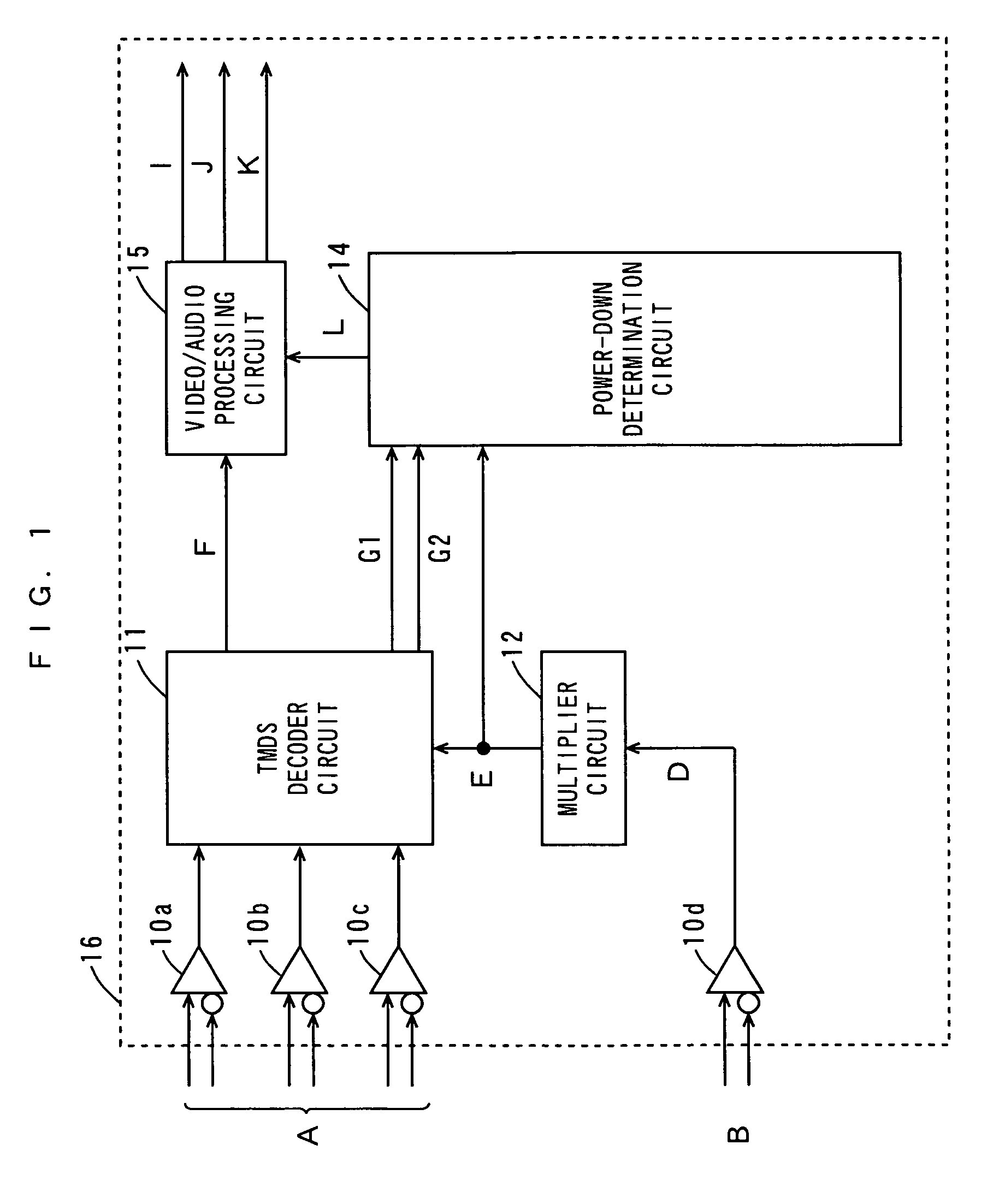
[0058]A first embodiment of the present invention will be described with reference to FIGS. 1 and 2.

[0059]FIG. 1 is a block diagram showing the structure of a high-speed digital interface decode receiver according to a first embodiment of the present invention.

[0060]The high-speed digital interface decode receiver (hereafter abbreviated to the interface decode receiver) in FIG. 1 includes differential buffers 10a, 10b, 10c, 10d, a TMDS decoder circuit 11, a multiplier circuit 12, a power-down determination circuit 14, and a video / audio processing circuit 15. The interface decode receiver, which is composed of a receiver LSI (Large Scale Integrated Circuit) 16, is mounted in the video display of a television receiver or the like.

[0061]The interface decode receiver is provided with digital signals in accordance with a high-speed digital interface standard, such as the HMDI standard or DVI standard, from source equipment. The source equipment includes, for example, a DVD (Digital Versa...

second embodiment

[0078]A second embodiment of the present invention will be described with reference to FIG. 3.

[0079]FIG. 3 is a block diagram showing the structure of a high-speed digital interface decode receiver according to a second embodiment of the present invention.

[0080]In the interface decoder receiver of FIG. 3, parts identical or corresponding to those in the interface decoder receiver of FIG. 1 are labeled with the identical symbols. The interface decode receiver of FIG. 3 differs from that shown in FIG. 1 as follows.

[0081]The interface decode receiver of FIG. 3 additionally comprise a counter circuit 13.

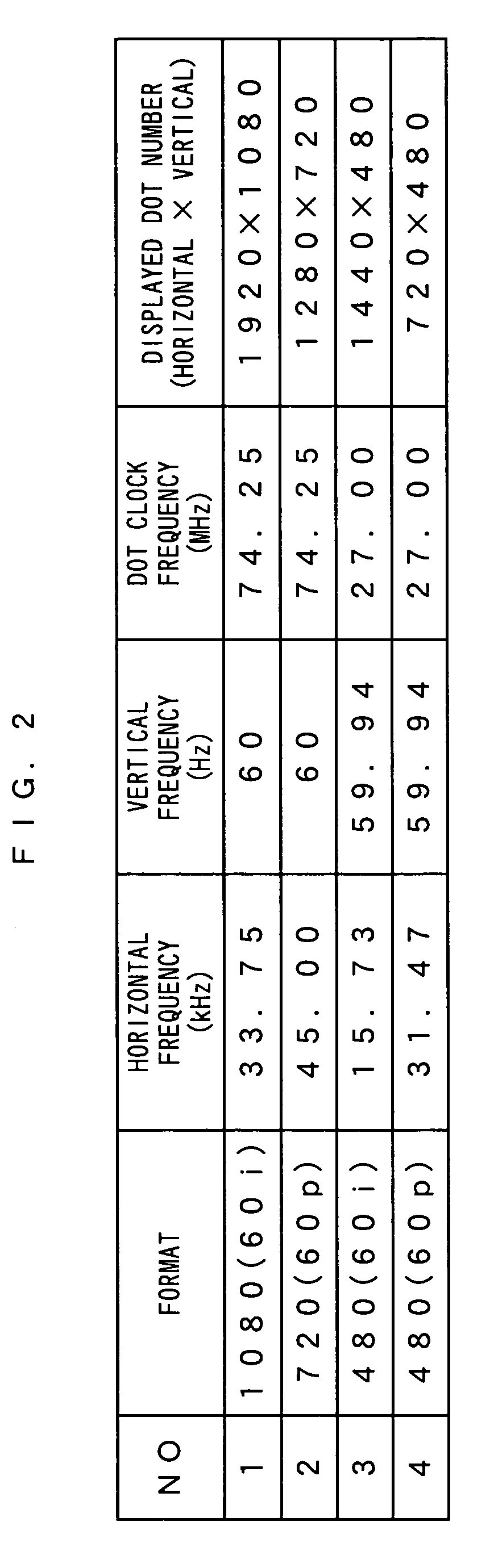
[0082]The counter circuit 13 is provided with a clock signal C having a certain frequency, which is input from a signal source 25 inside a video display, and also with a clock signal D output from the differential buffer 10d. The clock signal C has a lower frequency than that of the clock signal D.

[0083]The counter circuit 13 counts the number of pulses (clock number) of the clock signal...

third embodiment

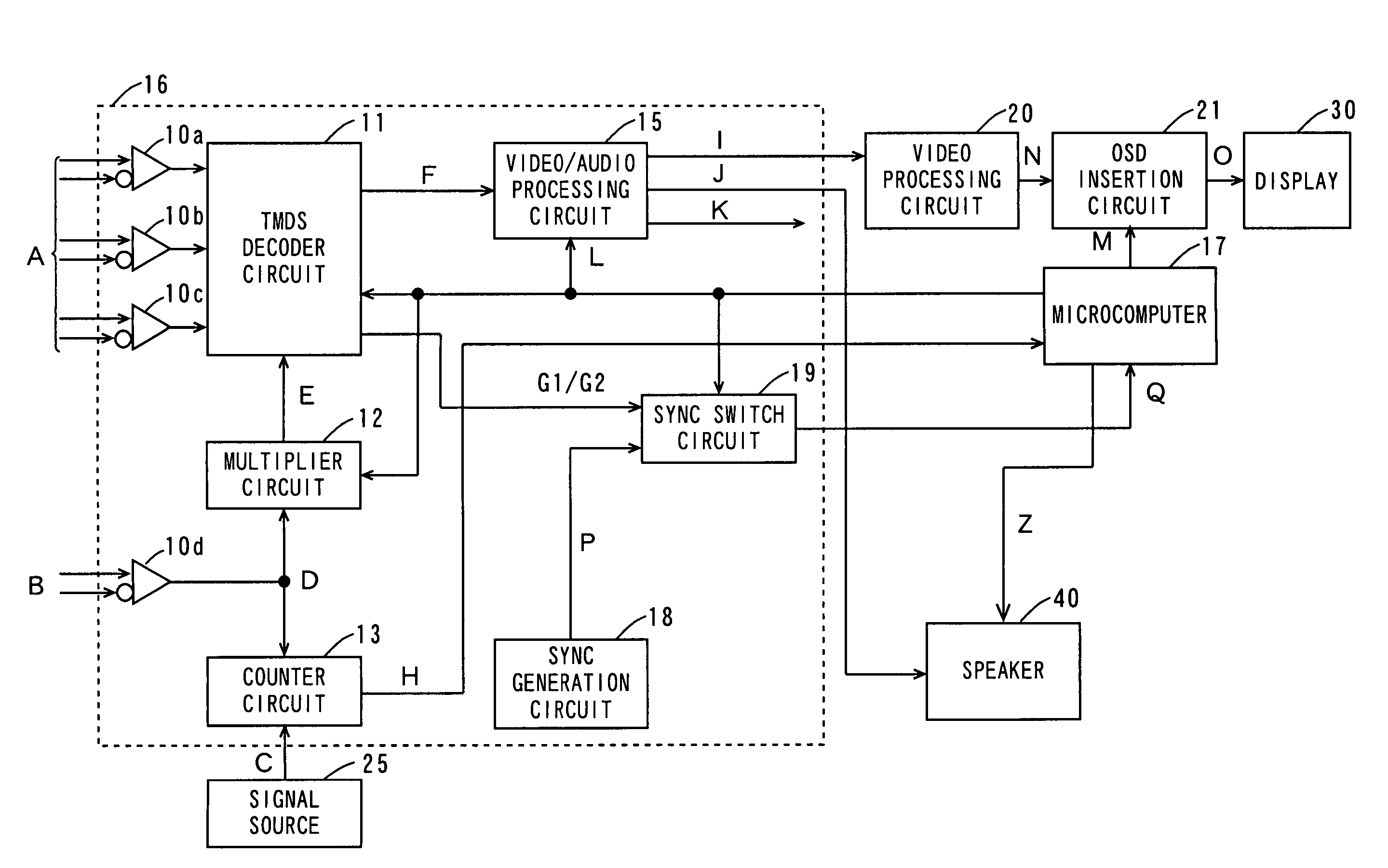
[0089]A third embodiment of the present invention will be described with reference to FIG. 4.

[0090]FIG. 4 is a block diagram showing the structure of a high-speed digital interface decode receiver according to a third embodiment of the present invention.

[0091]In the interface decoder receiver of FIG. 4, parts identical or corresponding to those in the interface decoder receiver of FIG. 3 are labeled with the identical symbols. The interface decode receiver of FIG. 4 differs from that shown in FIG. 3 as follows.

[0092]The interface decode receiver of FIG. 4 additionally comprise, instead of the power-down determination circuit 14 of FIG. 3, a microcomputer 17, a sync generation circuit 18, a sync switch circuit 19, a video processing circuit 20, and an OSD (On Screen Display) insertion circuit 21. The sync generation circuit 18 and sync switch circuit 19 are disposed internal to the receiver LSI 16.

[0093]The OSD insertion circuit 21 is connected with a display 30 including a CRT (Cath...


PUM


Abstract

A power-down determination circuit calculates the horizontal frequency and vertical frequency, respectively, employing a clock signal obtained from a multiplier circuit and horizontal synchronization signal and vertical synchronization signal obtained from a TMDS decode circuit. The power-down determination circuit then determines whether an input digital signal does or does not have a decodable video format by comparing the calculated horizontal frequency and vertical frequency with horizontal frequencies and vertical frequencies stored beforehand, for output of a power-down control signal indicative of the determination. Thus, in the case where the input digital signal does not have a decodable format, the power-down control signal controls a video / audio processing circuit to enter a power-down mode.

Description

TECHNICAL FIELD[0001]The present invention relates to a digital interface decode receiver that receives digital signals.BACKGROUND ART[0002]In recent years, the development of a variety of electronic equipment in accordance with high-speed digital interface standards, such as the HDMI (High Definition Multimedia Interface) standard or DVI (Digital Visual Interface) standard, is in progress (DDWG, “Digital Visual Interface,” Revision 1.0, Apr. 2, 1999, Internet <URL:http: / / www.ddwg.org / >). The HDMI standard, in particular, defines the transmission of an audio signal and control signal during the video blanking intervals. These high-speed digital interface standards adopt the so-called TMDS (Transmission Minimized Differential Signaling) serial transmission system.[0003]FIG. 6 is a block diagram showing an example of a conventional high-speed digital interface decode receiver. Referring to FIG. 6, the conventional high-speed digital will be described.[0004]In FIG. 6, the high-sp...

Claims


Application Information

Patent Timeline
Patent Type & Authority Patents(United States)
IPC IPC(8): H03K9/00G02B17/00G02B17/06G02B17/08G02B27/14G02B27/22H04N5/08H04N5/44H04N5/46H04N5/63H04N7/52
CPCH04N5/4401H04N21/4436H04N7/52H04N21/43632H04N5/08H04N5/46H04N5/63H04N21/426H04N21/434
Inventor GOTANDA, CHIKARANIO, YUTAKANAGATA, KOUICHIRO
Owner PANASONIC CORP
Why Eureka
Try Eureka