Semiconductor light-emitting device, semiconductor light-emitting module, and method of manufacturing the semiconductor light-emitting module

a light-emitting module and semiconductor technology, applied in semiconductor devices, semiconductor/solid-state device details, electrical devices, etc., can solve the problems of large heat generation, large amount of power consumption, insufficient green reproductivity, etc., and achieve high heat radiation property and heat resistance, high flexibility, and low cost

Inactive Publication Date: 2009-10-20
MAXELL HLDG LTD
View PDF12 Cites 30 Cited by
  • Summary
  • Abstract
  • Description
  • Claims
  • Application Information

AI Technical Summary

Benefits of technology

[0011]The present invention has been accomplished in view of the above problems of the related art. It is accordingly an object of the invention to provide a semiconductor device having high heat radiation property and heat resistance, and to provide a semiconductor module of a high flexibility, which can be manufactured at low cost, and a method of manufacturing the semiconductor module.

Problems solved by technology

In addition, one of the most important technical problem of the liquid crystal display panel is how to improve a brightness of an image.
In particular, a green reproductivity is insufficient.
Incidentally, the LED consumes a large amount of power and thus generates a large quantity of heat.
Accordingly, heat generated in the silicon submount cannot be efficiently released.
Moreover, there is a possibility that various problems resulting from the LED overheating, for example, deteriorations in characteristics occur.
This causes a problem in that a manufacturing process becomes completed and the module costs high.
This structure has a limitation on flexibility, and thus has a problem in that its application range is narrowed.

Method used


Image

  • Semiconductor light-emitting device, semiconductor light-emitting module, and method of manufacturing the semiconductor light-emitting module
  • Semiconductor light-emitting device, semiconductor light-emitting module, and method of manufacturing the semiconductor light-emitting module
  • Semiconductor light-emitting device, semiconductor light-emitting module, and method of manufacturing the semiconductor light-emitting module

Examples


Embodiment Construction

[0076]Exemplary embodiments of the present invention are described hereinafter with reference to the drawings. The description provided hereinbelow merely illustrates exemplary embodiments of the present invention, and the present invention is not limited to the below-described embodiments. The description hereinbelow is appropriately shortened and simplified to clarify the explanation. A person skilled in the art will be able to easily change, add, or modify various elements of the below-described embodiments, without departing from the scope of the present invention.

[0077]Hereinafter, an embodiment of a semiconductor device according to the present invention will be described with reference to the accompanying drawings. The following description is focused on a semiconductor light-emitting device by way of example.

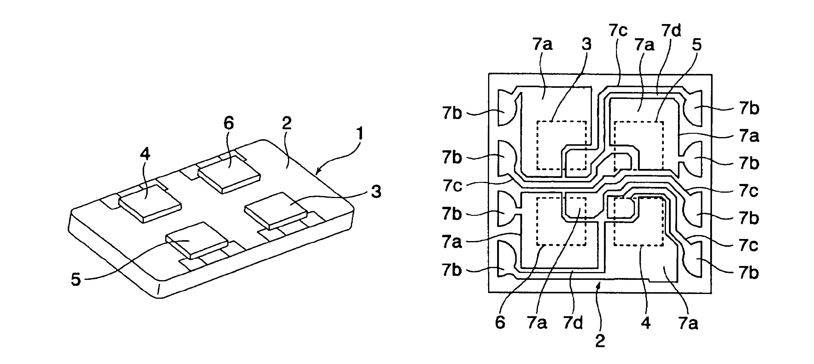
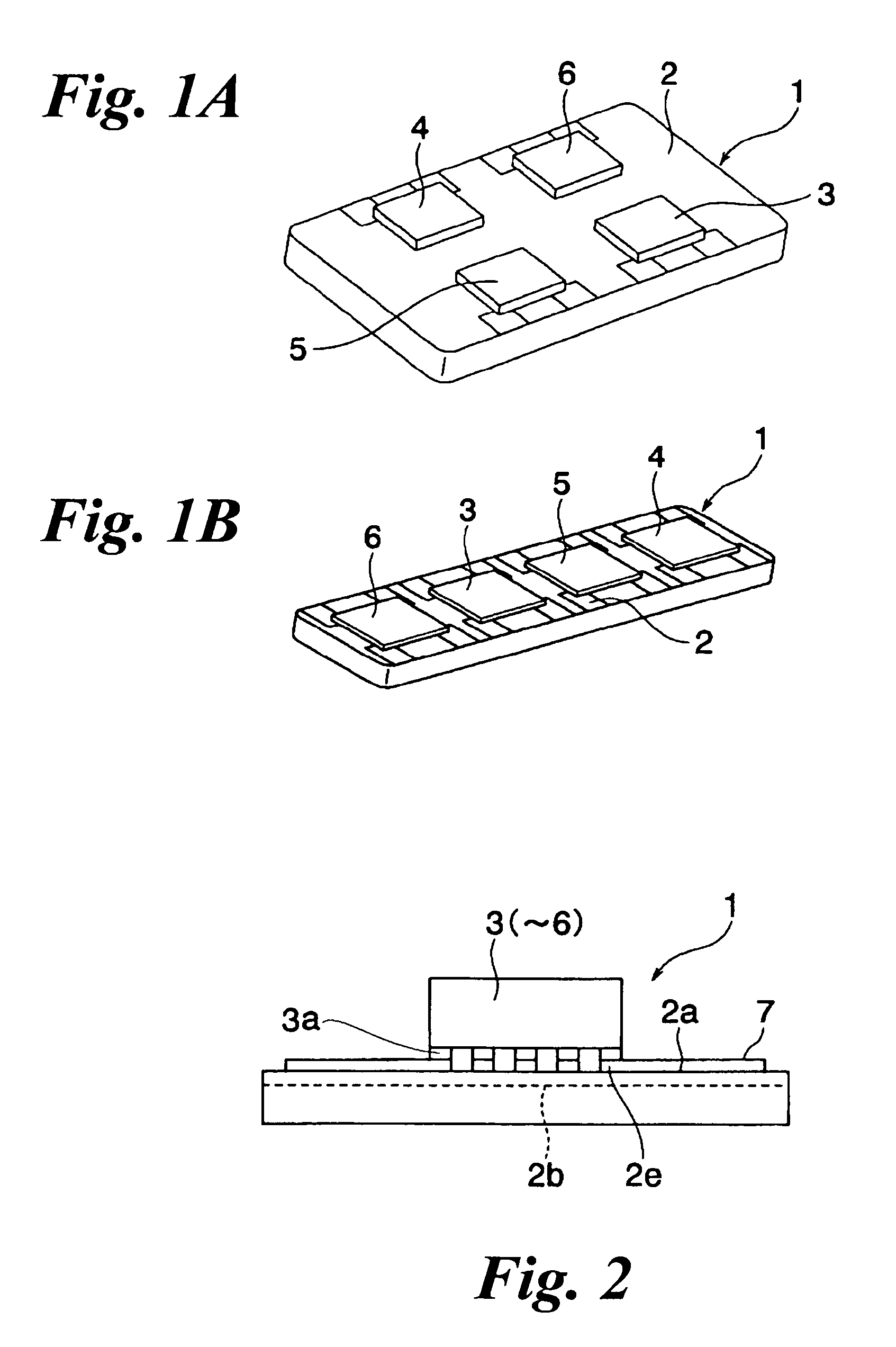
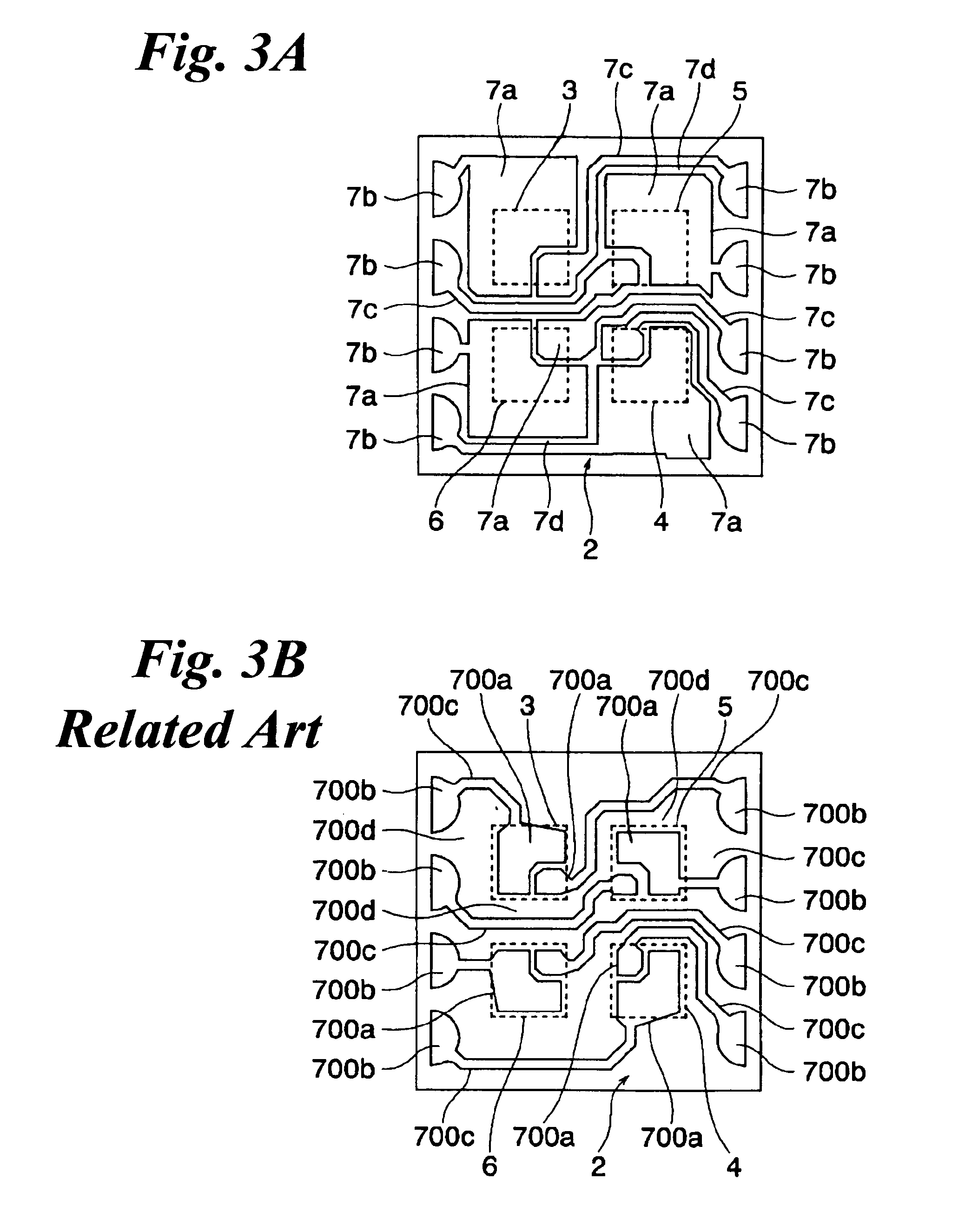
[0078]FIGS. 1A and 1B, and FIG. 2 are perspective views and a side view of a semiconductor light-emitting device of this embodiment, respectively. FIG. 3A is a plan view...


PUM


Abstract

A semiconductor light-emitting device according to an embodiment of the present invention includes chip LEDs formed on a silicon submount, in which a wiring pattern having a chip connecting terminal portion connecting the chip LEDs, an external connecting terminal portion connecting an external unit, and a plurality of lead portions connecting a corresponding chip connecting terminal portion and a corresponding external connecting terminal portion is formed on the silicon submount, and an area of the chip connecting terminal portions is made larger than an area of a region where the chip connecting terminal portion overlaps with the chip LEDs. Accordingly, a semiconductor light-emitting device of high heat radiation property and heat resistance can be provided.

Description

BACKGROUND OF THE INVENTION[0001]1. Field of the Invention[0002]The present invention relates to a semiconductor device obtained by mounting a semiconductor chip on a silicon submount, a semiconductor module, and a method of manufacturing the semiconductor module.[0003]2. Description of Related Art[0004]Up to now, large liquid crystal display panels have been applied to a liquid crystal display, a liquid crystal display television, or the like. In many cases, a cold-cathode tube has been used as a backlight of the display panel. In recent years, the use of the cold-cathode tube made of mercury has been avoided in order to overcome so-called RoHS for environmental protection. In addition, one of the most important technical problem of the liquid crystal display panel is how to improve a brightness of an image. From this viewpoint, in the case of using the cold-cathode tube, a color reproduction range is narrow. In particular, a green reproductivity is insufficient. Thus, the use of t...

Claims


Application Information

Patent Timeline
Patent Type & Authority Patents(United States)
IPC IPC(8): H01L23/495H01L23/12H01L33/60H01L33/64
CPCH01L23/147H01L23/5386H01L25/0753H01L2924/3025H01L33/641H01L2224/16H01L33/60
Inventor YAMANAKA, TOSHIHIROTSUKAMOTO, HIROYUKIKISHIMOTO, KIYOHARU
Owner MAXELL HLDG LTD
Why Eureka
Try Eureka