Sealed wafer packaging of microelectromechanical systems

a technology of microelectromechanical systems and wafers, which is applied in the direction of semiconductor devices, semiconductor/solid-state device details, electrical apparatus, etc., can solve the problems of device failure, introducing constraints, and dicing producing random particles that can contaminate and disable some microelectromechanical devices, so as to improve the registration of adhesive sheets

Active Publication Date: 2009-10-20
GENERAL ELECTRIC CO
View PDF22 Cites 14 Cited by
  • Summary
  • Abstract
  • Description
  • Claims
  • Application Information

AI Technical Summary

Benefits of technology

[0005]Another aspect of the invention resides in packaging MEMS devices using an adhesive sheet without additional adhesives to reduce the outgassing potential and at a low enough temperature to avoid damage to MEMS actuators.
[0021]Another aspect of the invention is the reduced stress build up due to thermal strain on the MEMS device due to the elastic modulus of the adhesive sheet being lower than the substrate.

Problems solved by technology

These devices generally require a controlled environment to operate for a long period of time.
Introduction of contaminants such as moisture, particulates or oxygen into the gas surrounding the device can cause sticking, contamination, or interference of the metal contacts, leading to device failure.
Dicing produces random particles that can contaminate and disable some of the microdevices.
However, these bonding materials produce an electrically conductive bond, which may introduce constraints as to how the wafers can be bonded and how the device layout may be configured.
However, this must be screen-printed onto one of the wafers, which can cause contamination of MEMS devices, it limits the process capability of through-wafer cavities and has the potential for outgassing over the operational lifetime of the device.

Method used


Image

  • Sealed wafer packaging of microelectromechanical systems
  • Sealed wafer packaging of microelectromechanical systems
  • Sealed wafer packaging of microelectromechanical systems

Examples


Embodiment Construction

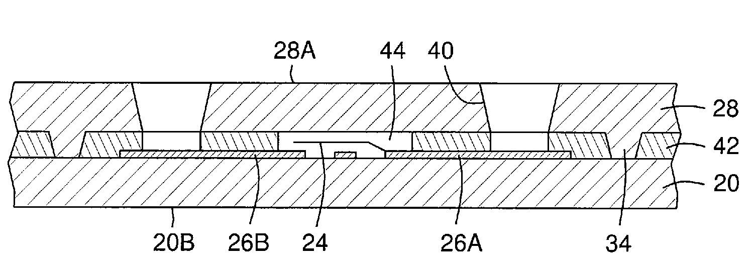
[0042]The present inventors have innovatively recognized that certain properties of an adhesive sheet embodying aspects of the present invention are conducive to an improved MEMS package and fabrication process, as will be described in greater detail below. In one example embodiment, the adhesive sheet can be a thermoplastic material. Some thermosets like epoxy or epoxy-based adhesives outgas during the cross-linking process. This gas can enter a MEMS device cavity, limiting control over the cavity environment. A thermoplastic does not need to cure, because there is no cross-linking involved with the bonding process. A thermoplastic also does not necessarily need an adhesive layer on either of the bonding surfaces. Some epoxies and other adhesives need such additional adhesive layer(s) to ensure proper bonding. The adhesive sheet is also an electrical insulator that enables passing electrical traces through the bond line without having to passivate them. The adhesive sheet can be fo...


PUM


Abstract

Multiple microelectromechanical systems (MEMS) on a substrate are capped with a cover using a layer that may function as a bonding agent, separation layer, and hermetic seal. A substrate has a first side with multiple MEMS devices. A cover is formed with through-holes for vias, and with standoff posts for layer registration and separation. An adhesive sheet is patterned with cutouts for the MEMS devices, vias, and standoff posts. The adhesive sheet is tacked to the cover, then placed on the MEMS substrate and heated to bond the layers. The via holes may be metalized with leads for circuit board connection. The MEMS units may be diced from the substrate after sealing, thus protecting them from contaminants.

Description

BACKGROUND[0001]The present invention relates to sealing and packaging of microelectromechanical fabricated devices on a device substrate before dicing.[0002]Microelectromechanical systems (MEMS) are miniaturized devices, such as microswitches that may range in size from about 1 micron to about 1 mm. These devices generally require a controlled environment to operate for a long period of time. Introduction of contaminants such as moisture, particulates or oxygen into the gas surrounding the device can cause sticking, contamination, or interference of the metal contacts, leading to device failure. MEMS devices are often manufactured in an array on a silicon wafer, and then separated or diced into individual units. Such separation is called “singulating”. Dicing produces random particles that can contaminate and disable some of the microdevices.[0003]There are known wafer-level packaging processes that may use bonding techniques such as a silicon / gold eutectic bond or gold / gold therma...

Claims


Application Information

Patent Timeline
Patent Type & Authority Patents(United States)
IPC IPC(8): H01L23/34B81C99/00
CPCB81C1/00269B81C2203/0118B81C2203/019B81C2203/032H01L2924/1461H01L2224/16225H01L2924/00B81B7/00B81C1/00
Inventor AIMI, MARCO FRANCESCOKAPUSTA, CHRISTOPHER JAMESGOWDA, ARUN VIRUPAKSHAHAYS, DAVID CECILBOOMHOWER, OLIVER CHARLESCLAYDON, GLENN SCOTTIANNOTTI, JOSEPH ALFREDKEIMEL, CHRISTOPHER FRED
Owner GENERAL ELECTRIC CO
Why Eureka
Try Eureka