Switchable resistive perovskite microelectronic device with multi-layer thin film structure

a resistive perovskite and microelectronic technology, applied in semiconductor devices, digital storage, instruments, etc., can solve the problem that the electric field or pulsed current through the sample cannot create a high enough magnetic induction, and achieve the effect of reducing the pulse voltage needed to switch the device, increasing the asymmetric configuration and magnifying the resistance switching region

Active Publication Date: 2009-10-27
UNIV HOUSTON SYST
View PDF6 Cites 69 Cited by
  • Summary
  • Abstract
  • Description
  • Claims
  • Application Information

AI Technical Summary

Benefits of technology

[0011]A buffered electric-pulse-induced-resistance change device (buffered-EPIR device) is provided. The buffered-EPIR device comprises a conductive bottom electrode overlying the substrate, a top conductive electrode, a perovskite active layer, and a buffer layer interposed between the perovskite function layer and an electrode, and two or more buffer layers inserted between two sides of perovskite function layer and two electrodes respectively, in the devices. The resistance of the perovskite function layer can be modified by electrical pulses and / or applied DC potentials, and thus such layer is a perovskite switchable function layer. The buffer layer material can be either a non-switchable or switchable material. By adding the buffer layers, the device changes from a device having a structure of electrode / perovskite / electrode, an EPIR device, to a device having a structure of electrode / buffer / perovskite / buffer / electrode, a buffered-EPIR device. The buffered-EPIR device can be fabricated on various substrates such as oxides, semiconductors, and integrated circuit wafer substrates. The benefits of the buffer layers to the device include, but are not limited to, an increased asymmetric configuration and magnifying resistance switching region, reduction of the pulse voltage needed to switch the device, protection of the device from being damaged by a large pulse shock, improvement of the temperature properties and radiation hardness, increased device stability, and improvement of switching to multiple resistance states. The electrical pulse may have square, saw-toothed, triangular, sine, oscillating or other waveforms, and may be of positive or negative polarity. Multiple pulses may be applied to the material to produce incremental changes in properties of the buffered-EPIR device.

Problems solved by technology

The pulsed electric field or pulsed current through the sample cannot create a high enough magnetic induction to change the resistance of the PCMO.

Method used


Image

  • Switchable resistive perovskite microelectronic device with multi-layer thin film structure
  • Switchable resistive perovskite microelectronic device with multi-layer thin film structure
  • Switchable resistive perovskite microelectronic device with multi-layer thin film structure

Examples


Embodiment Construction

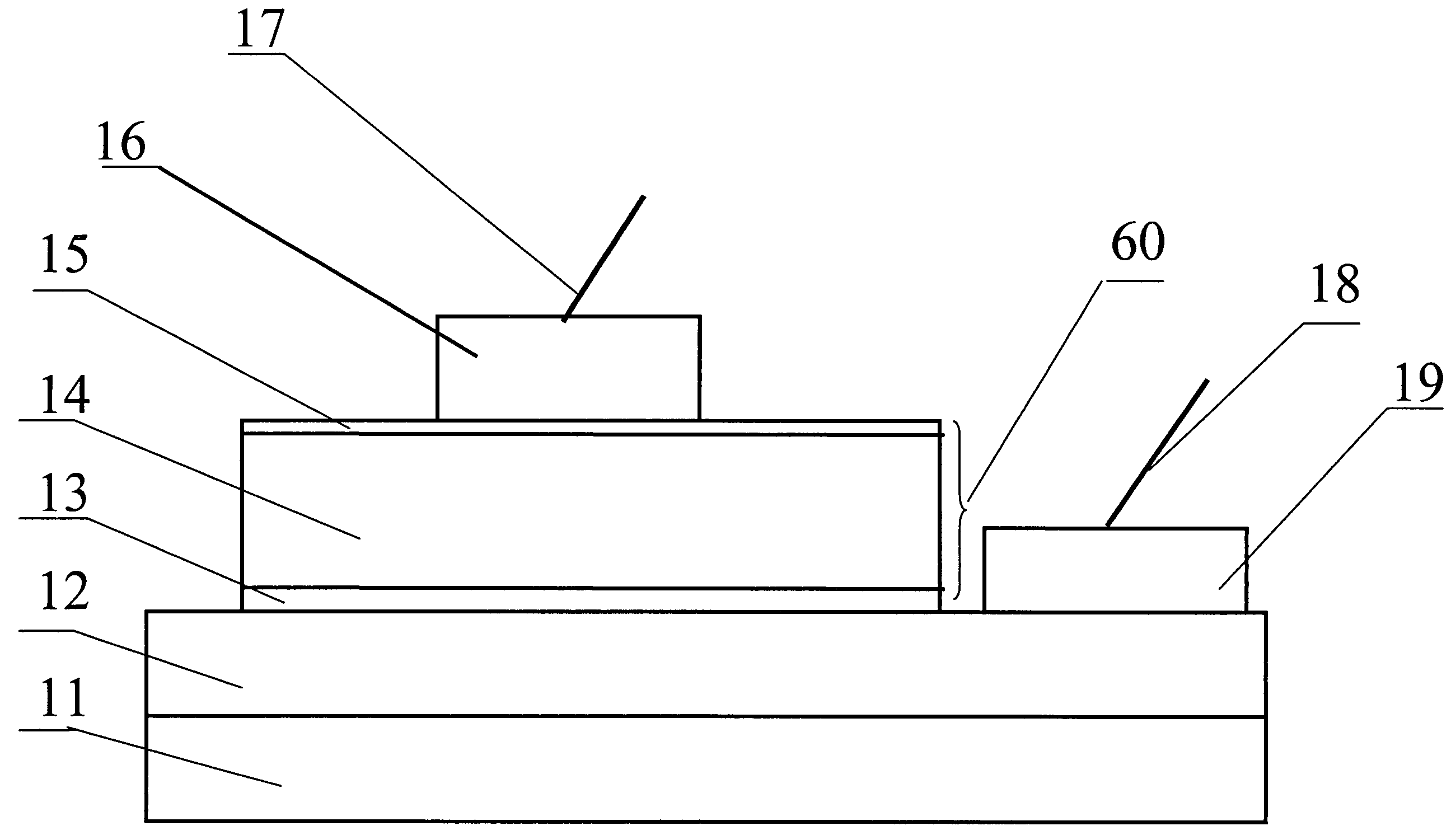
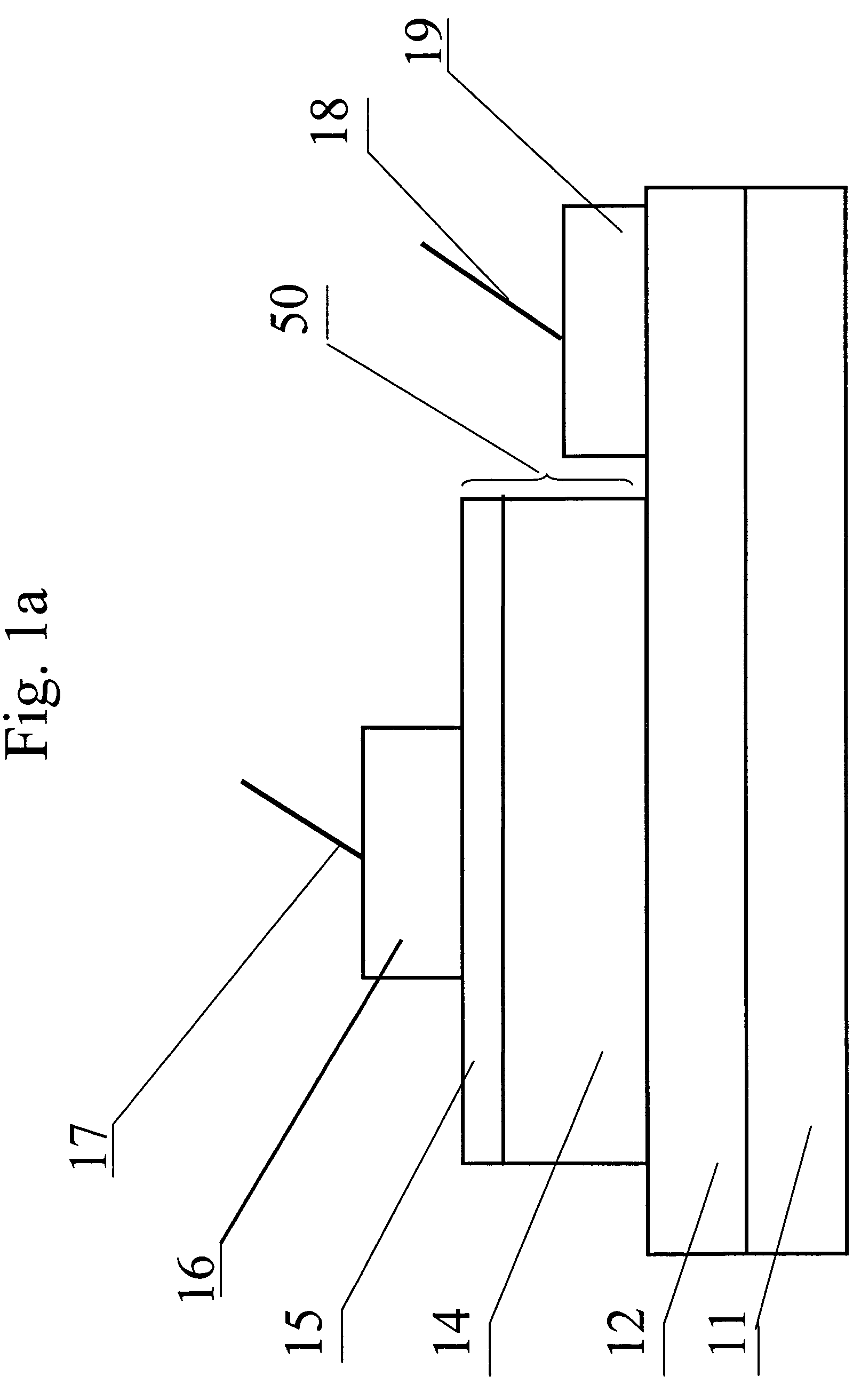
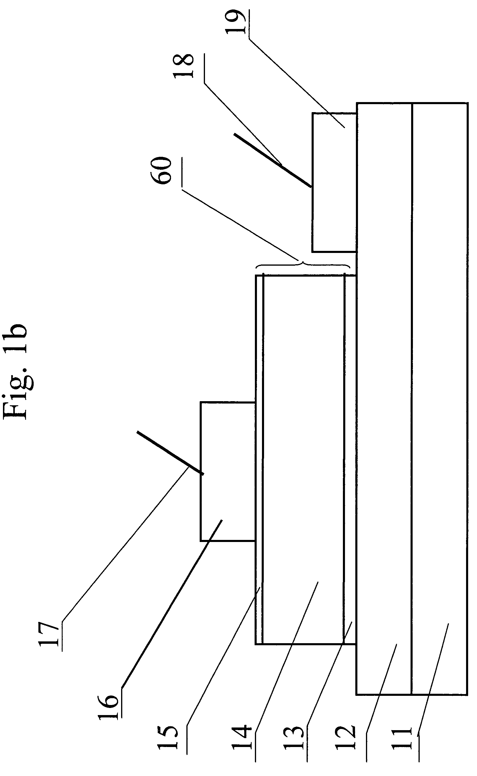
[0020]In summary, buffer layers are added to an EPIR device to create a buffered-EPIR device. Referring to FIG. 1a, a bottom conductive electrode layer 12 is used as the bottom electrode layer on substrate 11. A thin top switchable function film, or layer, 14 partially covers the bottom conductive electrode layer 12. A bottom electrode contact pad 19 is connected to the bottom conductive electrode layer 12. The top switchable function layer 14 is covered with a top buffer layer 15. The top switchable function layer 14 and top buffer layer 15 form a multi-layer structure 50. A top electrode contact pad 16 is fabricated on top of the top buffer layer 15. Electrode contact pads 16 and 19 are connected to wires 17 and 18, respectively. The conductive electrode layer 12 and the top electrode contact pad 16 may be crystalline or polycrystalline conducting oxide or metallic layers.

[0021]Referring to FIG. 1b, the individual components and their arrangements in the buffered-EPIR device with ...


PUM


Abstract

A switchable resistive device has a multi-layer thin film structure interposed between an upper conductive electrode and a lower conductive electrode. The multi-layer thin film structure comprises a perovskite layer with one buffer layer on one side of the perovskite layer, or a perovskite layer with buffer layers on both sides of the perovskite layer. Reversible resistance changes are induced in the device under applied electrical pulses. The resistance changes of the device are retained after applied electric pulses. The functions of the buffer layer(s) added to the device include magnification of the resistance switching region, reduction of the pulse voltage needed to switch the device, protection of the device from being damaged by a large pulse shock, improvement of the temperature and radiation properties, and increased stability of the device allowing for multivalued memory applications.

Description

CROSS-REFERENCE TO RELATED APPLICATIONS[0001]This application claims the benefit of the following U.S. Provisional Application: No. 60 / 536,155, filed Jan. 13, 2004.STATEMENT REGARDING FEDERALLY SPONSORED RESEARCH OR DEVELOPMENT[0002]Not Applicable.REFERENCE TO A “SEQUENTIAL LISTING,” A TABLE, OR A COMPUTER PROGRAM LISTING APPENDIX SUBMITTED ON A COMPACT DISC[0003]Not Applicable.BACKGROUND OF THE INVENTION[0004]1. Field of the Invention[0005]The present invention relates to a two-terminal microelectronic device, and, in particular, to a two-terminal non-volatile resistor device, having a structure of electrode / perovskite-active-material-layer / electrode, which is an Electric-Pulse-Induced-Resistance change device, commonly referred to by the acronym EPIR.[0006]2. Description of the Related Art[0007]The properties of materials having a perovskite structure, among them colossal magneto-resistance (CMR) materials and high transition temperature superconductivity (HTSC) materials, can be ...

Claims


Application Information

Patent Timeline
Patent Type & Authority Patents(United States)
IPC IPC(8): H01L21/00H01L29/76H01C7/00H01L45/00
CPCG11C13/0007G11C2213/31H01C7/006H10N70/801H10N70/20H10N70/8836H10N70/826
Inventor WU, NAIJUANCHEN, XINIGNATIEV, ALEX
Owner UNIV HOUSTON SYST
Why Eureka
Try Eureka