
Semiconductor integrated circuit device and storage apparatus having the same

a technology of integrated circuit and storage apparatus, which is applied in the direction of logic circuits, pulse techniques, and increasing modifications, etc., can solve the problems of inability to change the replacement target logical block, the cost of reproducing asics is extremely high, and the time required for asics development has increased, etc., to achieve the effect of simple connection between the first large scale integrated circuit and the programmable second large scale integrated circuit, high reliability and low number of connection pins

Active Publication Date: 2009-10-27
RAKUTEN GRP INC
View PDF2 Cites 13 Cited by
  • Summary
  • Abstract
  • Description
  • Claims
  • Application Information

AI Technical Summary

Benefits of technology

[0018]The semiconductor integrated circuit device having the above configuration has high reliability because, even when a failure is detected in one of a plurality of first logical blocks during the operation of the first large scale integrated circuit, the first large scale integrated circuit does not have to stop, and so the semiconductor integrated circuit device can continue its operation.
[0019]Moreover, because the connection between the first large scale integrated circuit and the programmable second large scale integrated circuit is simplified, the number of connection pins is small, the size of the semiconductor integrated circuit device can be reduced while minimizing the effects of the number of connection pins on the chip size or package size, and so the semiconductor integrated circuit device can be manufactured at small cost.
[0021]Accordingly, the storage apparatus having the above configuration has a high reliability because, even when a failure is detected in one of a plurality of first logical blocks during the operation of the first large scale integrated circuit, the first large scale integrated circuit does not have to stop, and so the storage apparatus can continue its operation.
[0022]According to the invention, it is possible to provide a semiconductor integrated circuit device capable of continuing its operation even when a failure is detected in its logical block(s) during the operation of a first large scale integrated circuit, and a storage apparatus including that semiconductor integrated circuit device.
[0023]Moreover, because the connection between the first large scale integrated circuit and the programmable second large scale integrated circuit is simplified, the number of connection pins is small, the size of the semiconductor integrated circuit device can be reduced while minimizing the effect of the chip size or package size, and so the semiconductor integrated circuit device can be manufactured at small cost.

Problems solved by technology

In recent years, the cost and time required for the development of ASICs have increased due to the subdivided processes, accordingly, the cost for reproducing ASICs is extremely high.
Moreover, regarding a self-test function, self-test and replacement of a faulty logical block with a FPGA are performed only when an ASIC is not operating, for example, when the ASIC is powered on, so the replacement target logical block cannot be changed during operation of the ASIC.
Due to the subdivided manufacturing processes for semiconductor integrated circuits, minute dust attached to ASICs during manufacture can be the cause of a failure.
Due to the subdivided manufacturing processes, the degree of integration of transistors and wires in ASICs has been raised and minute dust, which could not be a problem in the conventional processes, can cause a failure in the ASICs.
Furthermore, some failures in ASICs may be caused due to the situation where although the ASICs are operating normally in the beginning, after power being applied for a while, a short or break in the wiring in the ASICs occurs.
In that case, the result of the self-test is normal, but in fact a failure has occurred.
However, the ASICs cannot perform normal operation during self-test, so they have to halt normal operation to enable their self-test functions.
Accordingly, frequent performance of self-test during ASIC operation may cause performance deterioration in ASICs.
For example, the ASICs arranged in storage apparatuses are mainly in charge of data transfer and, if a self-test is performed during data transfer, performance deteriorates, i.e., transfer speed slows down.
Consequently, the entire performance of the storage apparatuses degrades.
Accordingly, stopping the operation of ASICs to perform self-test is not realistic.
Also, because the self-test function is not perfect, some existing failures may be missed.
For example, some failures occur only when data is transferred with special timing or when a special pattern is transferred, and the self-test function cannot detect those failures.

Method used


Image

  • Semiconductor integrated circuit device and storage apparatus having the same
  • Semiconductor integrated circuit device and storage apparatus having the same
  • Semiconductor integrated circuit device and storage apparatus having the same

Examples


embodiment 1

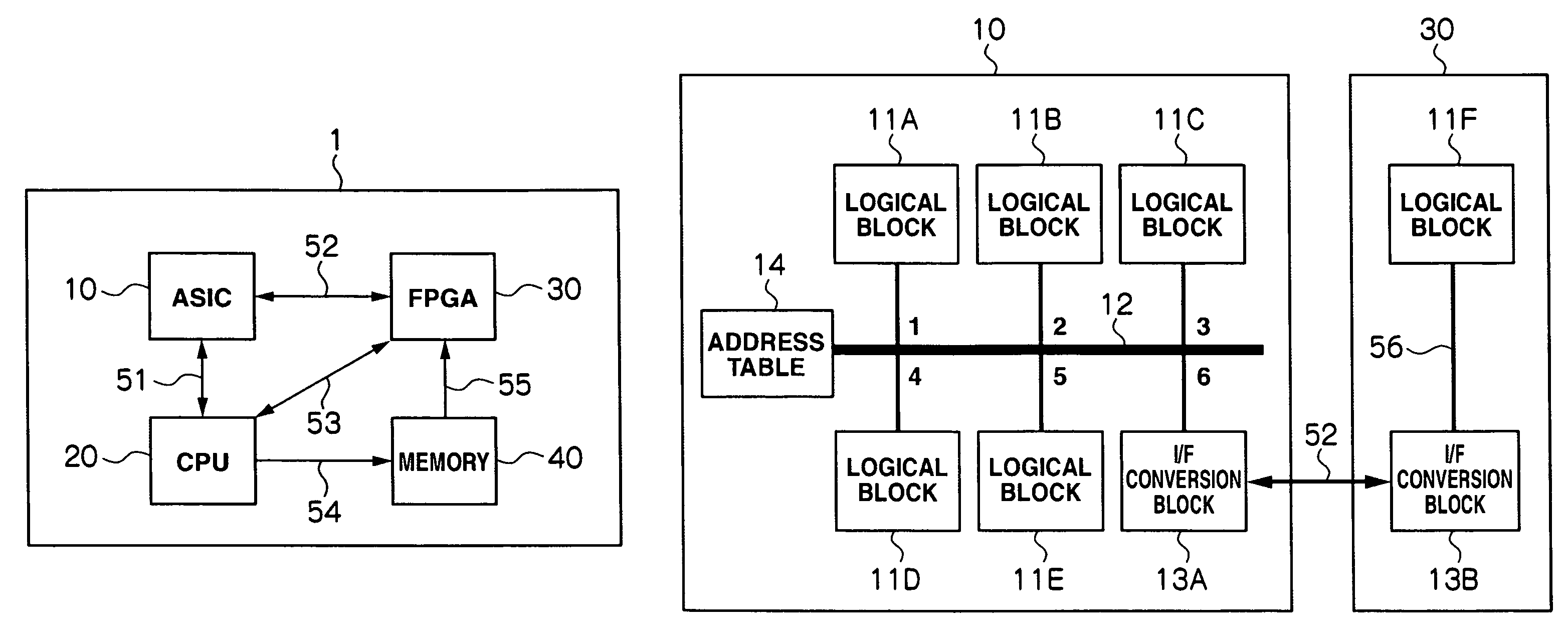
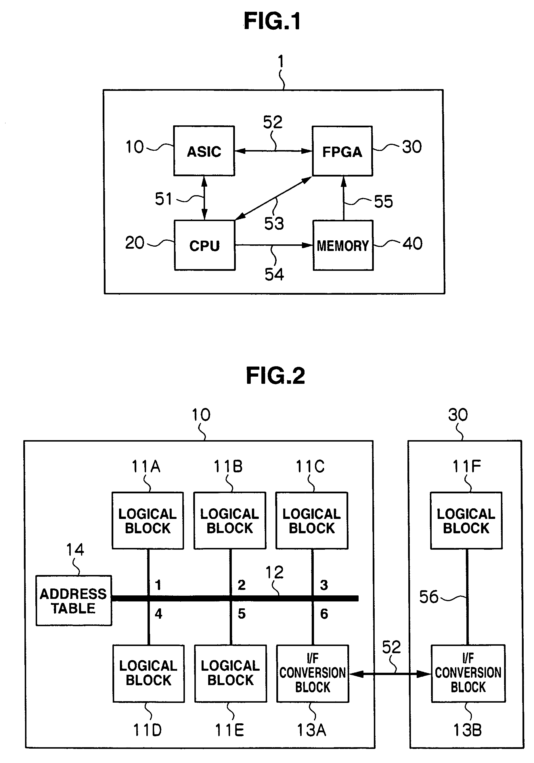
[0051]FIG. 1 shows the configuration of a built-in ASIC board 1, which is a semiconductor integrated circuit device. An ASIC 10, CPU 20, FPGA 30, and memory 40 are arranged on the built-in ASIC board 1. The CPU 20 is connected to the ASIC 10 and FPGA 30 with signal lines 51 and 53 respectively, thereby enabling data exchange. The CPU 20 is also connected to the memory 40 with a signal line 54, thereby enabling data transmission to the memory 40. The memory 40 and FPGA 30 are connected to each other with a signal line 55, thereby enabling data transmission from the memory 40 to the FPGA 30. The ASIC 10 and FPGA 30 are also connected to each other with a signal line 52, thereby enabling data exchange.

[0052]The ASIC 10 is a first large scale integrated circuit and includes circuits for performing various tasks. The CPU 20 controls the ASIC 10, FPGA 30, and memory 40, thereby controlling the entire built-in ASIC board 1. The FPGA 30 is a programmable second large scale integrated circui...

embodiment 2

[0085]Embodiment 2 of the invention will be explained below. Conventionally, data in a RAM or a flip-flop is corrupted due to irradiation of alpha rays or neutron rays, for example, a data element originally having ‘0’ may have ‘1’ instead. In recent years, in particular, the RAM and flip-flop are manufactured in small sizes thanks to subdivided manufacturing processes, and so the data may be corrupted even by smaller energy. This is called a soft error and, because it is not a failure in the hardware, normal operation can be continued as long as another piece of correct data is written in the RAM or flip-flop.

[0086]In embodiment 1, when a failure is detected, even when the failure is caused by a soft error, not a hard error, the failure is handled as a hard error and a faulty logical block is replaced with the logical block 11F in the FPGA 30. However, if the failure is not caused by a physical failure in the ASIC 10, it is unnecessary to use the FPGA 30 and the built-in ASIC board...

embodiment 3

[0097]Embodiment 3 of the invention will be explained below. The configurations in embodiments 1 and 2 include the I / F conversion blocks 13A and 13B; however, the configuration in embodiment 3 has no I / F conversion block 13A or 13B. Only the differences from embodiments 1 and 2 will be explained below and shown in the drawing.

[0098]FIG. 13 shows the configurations of the ASIC 10 and FPGA 30 in embodiment 3. The internal bus 12 in the ASIC 10 is directly connected to the logical block 11F in the FPGA 30. The processing performed by the ASIC 10 and CPU 20 is the same as that in embodiments 1 and 2. Note that the self-test circuits 15A-15E used in embodiment 2 are not shown in FIG. 13.

[0099]According to embodiment 3, unlike in embodiments 1 and 2, it is not necessary to provide the I / F conversion blocks 13A and 13B, so it is possible to obtain a built-in ASIC board 1 where the ASIC 10 and the FPGA 30 are easily connected.


PUM


Abstract

A semiconductor integrated circuit device includes: a first large scale integrated circuit including a plurality of first logical blocks; a programmable second large scale integrated circuit connected the first large scale integrated circuit and including a second logical block; a memory storing data for achieving the purposes of the first logical blocks; and a control unit that, when a failure is detected in any of the first logical blocks during the operation of the first large scale integrated circuit, writes the data for the faulty first logical block stored in the memory to the second logical block, and uses the second logical block in place of the faulty first logical block.

Description

CROSS-REFERENCES TO RELATED APPLICATIONS[0001]This application relates to and claims priority from Japanese Patent Application No. 2007-233103, filed on Sep. 7, 2007, the entire disclosure of which is incorporated herein by reference.BACKGROUND[0002]1. Field of the Invention[0003]The present invention relates to a semiconductor integrated circuit device and storage apparatus, and is particularly suitable for use in a semiconductor integrated device enabling normal device operation even when a failure occurs in a large scale integrated circuit, by using another programmable large scale integrated circuit, and a semiconductor integrated circuit device having such a semiconductor integrated circuit device.[0004]2. Description of Related Art[0005]With the development in semiconductor technology, manufacturing processes for semiconductor integrated circuits called LSI (Large Scale Integration circuit) or ASIC (Application Specific Integrated Circuit) have been subdivided to enhance the i...

Claims


Application Information

Patent Timeline
Patent Type & Authority Patents(United States)
IPC IPC(8): H03K19/003H03K19/00
CPCG06F11/142G06F11/2089G06F11/201G06F11/2005
Inventor FUSEYA, TOMOKATSU
Owner RAKUTEN GRP INC
Learn More