
Method and device for 3D imaging

a 3d imaging and imaging method technology, applied in the field of 3d imaging, can solve the problems of electromagnetic interference between different components of electronic car equipment, and the electronic car equipment developers are increasingly faced with the problem of electromagnetic interference, so as to improve detection robustness, reduce the peak, and improve the effect of electromagnetic compatibility

Active Publication Date: 2009-10-27
IEE INT ELECTRONICS & ENG SA
View PDF6 Cites 2 Cited by
  • Summary
  • Abstract
  • Description
  • Claims
  • Application Information

AI Technical Summary

Benefits of technology

The invention provides an improved method for 3D imaging of an actively illuminated scene by emitting intensity-modulated light and detecting the scattered and / or reflected light using an imaging sensor. The modulation frequency is varied over the integration time interval, resulting in a broader frequency range and lower peak power, which improves electromagnetic compatibility with electronic devices in the surrounding area. The method also allows for more robust phase detection in the presence of other illumination devices with the same frequency spectrum. The invention further relates to a 3D imaging system comprising signal generation means for generating a modulation signal with a varying modulation frequency, an illumination unit for emitting the modulated light, an imaging sensor for detecting the scattered and / or reflected light, and an evaluation unit for calculating distance information. The signal generation means can be a voltage-controlled oscillator, a numerically controlled oscillator, or a multiplexer, which can switch between different values of the modulation frequency. A frequency average builder can provide the average frequency of the modulation frequency based on a control signal.

Problems solved by technology

Especially in the automotive field, electronics developers are increasingly faced with the problem of electromagnetic interference between different components of electronic car equipment.

Method used


Image

  • Method and device for 3D imaging
  • Method and device for 3D imaging

Examples


Embodiment Construction

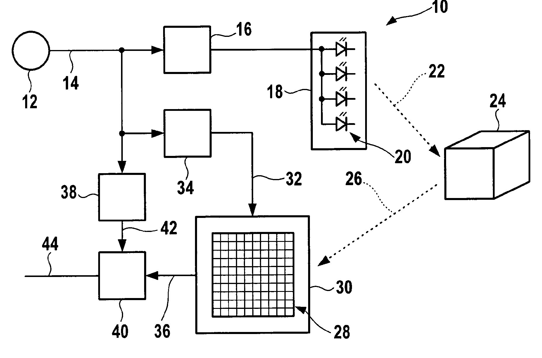
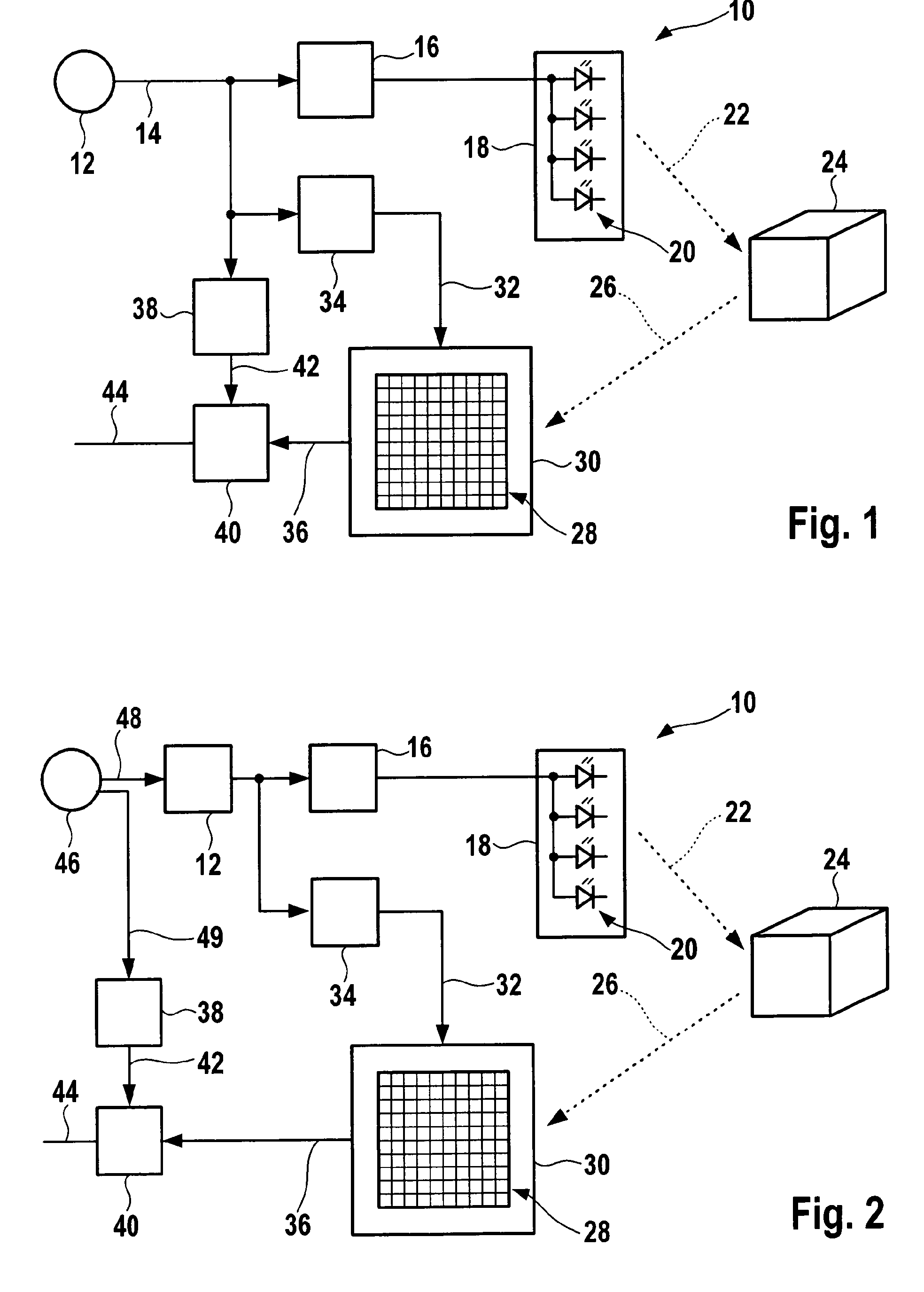
[0013]In the 3D imaging system 10 shown in FIG. 1, signal source 12 generates on its output a modulation signal 14 with a variable frequency. The signal source 1 is in this case a voltage-controlled oscillator (VCO) running at a carrier frequency and controlled by a defined signal that varies this frequency. The signal source 12 is connected to the illumination unit, which comprises an illumination driver 16 and a light source 18.

[0014]The illumination driver 16 amplifies the modulation signal 14 to drive the several individual light emitting devices 20 of the light source 18. The light source 18 emits an intensity-modulated light wave 22 into the target region, which contains an object 24 to be measured. Light is scattered or reflected on the surface of object 24 and a fraction 26 of the scattered / reflected light is directed onto the pixel array 28 of the three-dimensionally sensitive imager 30. The imager 30 (camera) is at the same time fed with a demodulation signal 32, which is ...


PUM


Abstract

A method for 3D imaging of an actively illuminated target region includes emitting intensity-modulated light at a variable modulation frequency into the target region, the emitted light is scattered / reflected in the target region depending on the optical properties of the objects or beings present therein, a scattered and / or reflected fraction of the light is detected during an integration time interval by phase-sensitive integration in each pixel of an imaging sensor, the modulation phase between the emitted and the detected light is determined and spatially resolved, and distance information is calculated based on the spatially resolved modulation phase and an average frequency of the modulation frequency.

Description

TECHNICAL FIELD[0001]The present invention generally relates to 3D imaging, more specifically to 3D imaging based on spatially resolved phase detection of modulated light waves.BRIEF DISCUSSION OF RELATED ART[0002]As opposed to conventional 2D imaging, a 3D imaging system requires depth information about the target scene, i.e. the distances between one or more observed objects and an optical receiver of the system need to be determined. The basic principles of three-dimensional imagers are described in detail in EP 1 152 261 A1 and WO 98 / 10255. 3D imaging systems of this kind use active illumination of the scene with intensity-modulated light. The scene is optically imaged onto a two-dimensional pixel array. Each pixel detects the modulation phase of the light that has been emitted by the illumination device and reflected or scattered from an object of the scene to the pixel. From this phase, the time lapsed between transmission and echo-return of the transmitted light and hence the...

Claims


Application Information

Patent Timeline
Patent Type & Authority Patents(United States)
IPC IPC(8): G01C3/08G01S17/894
CPCG01S17/89G01S17/36G01S17/894
Inventor WATGEN, CLAUDELAMESCH, LAURENT
Owner IEE INT ELECTRONICS & ENG SA
Learn More