
Halogen-resistant, anodized aluminum for use in semiconductor processing apparatus

a technology of anodized aluminum and semiconductor processing equipment, which is applied in the direction of electrolytic coatings, surface reaction electrolytic coatings, coatings, etc., can solve the problems of reducing affecting the performance etc., to achieve the effect of improving the performance life of anodized semiconductor equipment, improving abrasion resistance, and generalized density

Inactive Publication Date: 2006-04-25
APPLIED MATERIALS INC
View PDF20 Cites 18 Cited by
  • Summary
  • Abstract
  • Description
  • Claims
  • Application Information

AI Technical Summary

Benefits of technology

[0023]The LP™ aluminum alloy, in sheet or extruded or forged form, or after pre-machining into a desired shape, is typically stress relieved at a temperature of about 330° C. or less, prior to creation of an aluminum oxide protective film over the article surface. This stress relief provides a more stable surface for application of the aluminum oxide protective film. When the LPT aluminum alloy article is machined from a block of material, it is advantageous to stress relieve the block of material after machining, to relieve stress resulting from the machining operation. We have discovered that it is very important to heat relieve thermal stress in the LP™ aluminum alloy using lower peak temperatures than commonly recommended for aluminum alloys. Employment of a peak stress relief temperature of less than about 330° C. will minimize the undesirable precipitation of impurities at the aluminum grain boundaries and eliminate unwanted aluminum grain growth. This ensures the desired material properties of the alloy with respect to grain structure, non-aluminum metal (mobile and nonmobile impurity) distribution, and mechanical properties in the article produced. By controlling the grain size of the aluminum alloy, the distribution of mobile and nonmobile impurities within the alloy, and the residual stress within the article to be anodized, the interface between a protective aluminum oxide film and the underlying aluminum alloy provides a uniform transition from one crystal structure to another, improving the performance and lifetime of the article.
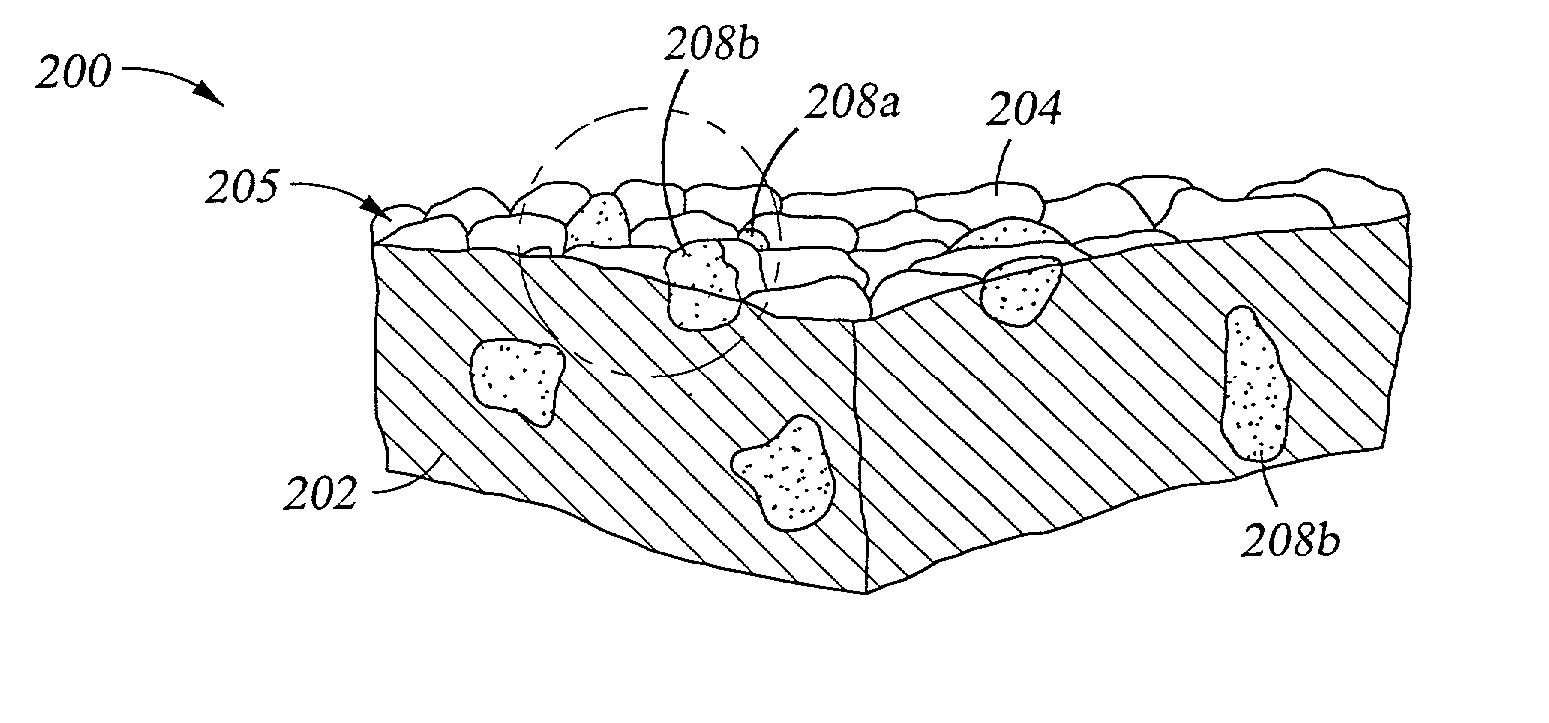
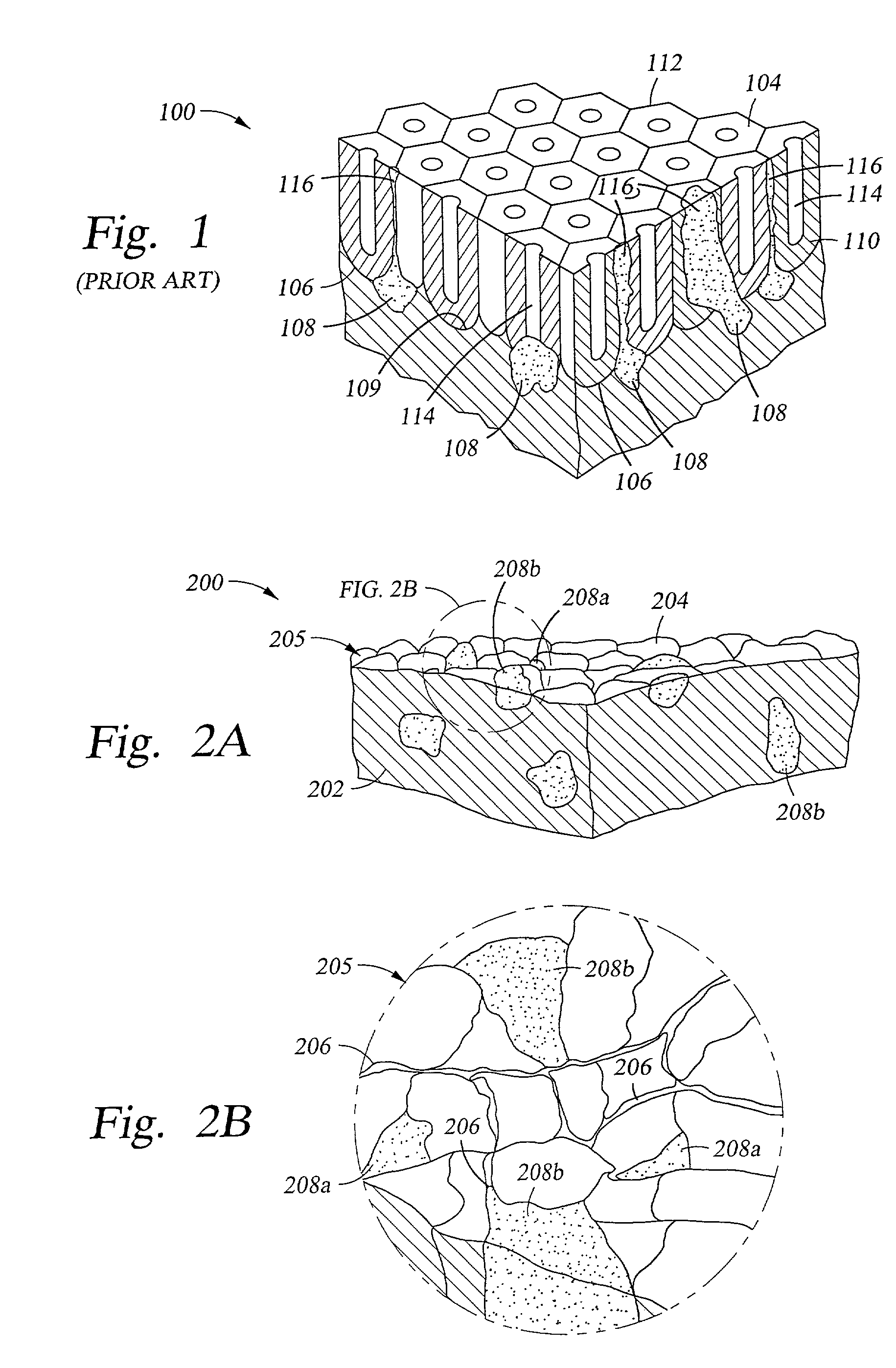
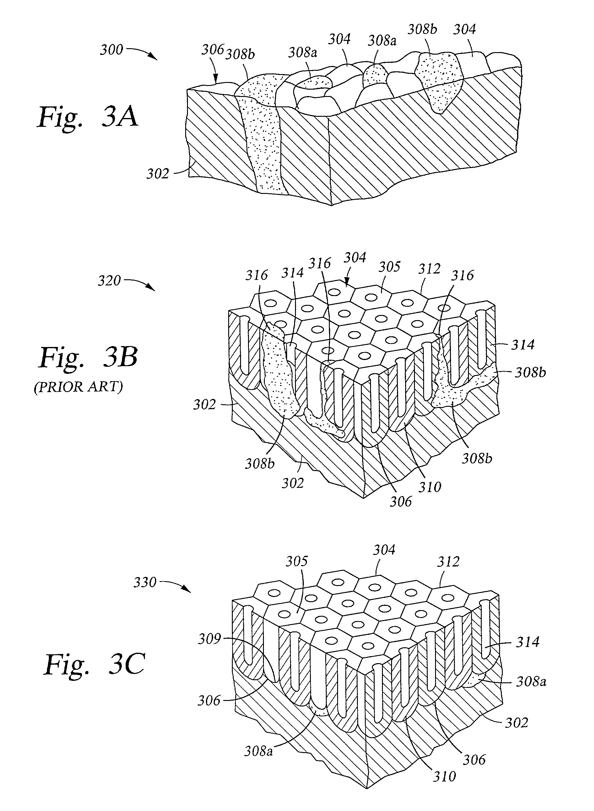
[0027]The particular combination of process variables described above also produces an oxidized aluminum layer which is more densely packed and more uniform than previously known in the art. For example, the size of the internal pores (shown as 314 on FIG. 3C) within the hexagonal cells of the oxidized aluminum film of the present invention range in size from about 300 Å to about 700 Å. This is compared with previously known oxidized aluminum films, where the pore size varied from about 100 Å to about 2000 Å in diameter. As a result, the density of the present oxidized film is generally higher, providing improved abrasion resistance. Depending on the application, the normal range of the anodized film thickness ranges between about 0.7 mils to about 2.5 mils (18 μm to 63 μm).
[0028]Although the above anodization process is beneficial for any article formed from the specialized halogen-resistant aluminum alloy article described in the Bercaw et al. patents, it is particularly beneficial when the aluminum alloy is LP™. In addition, when the halogen-resistant aluminum article is heat-treated for stress relief at a temperature of less than about 330° C., the performance lifetime of the anodized semiconductor apparatus is further improved. The best-performing anodized aluminum alloy article is one formed from LP™ alloy which has been heat-treated at temperatures below about 330° C., and which has an electrochemically applied aluminum oxide protective film. The quality of the protective coating is further improved when the alloy article surface is cleaned prior to anodization, as previously described.

Problems solved by technology

In addition, since the processes used to create the integrated circuits leave contaminant deposits on the surfaces of the processing apparatus, such deposits are commonly removed using plasma cleaning techniques which employ at least one halogen-containing gas.
However, aluminum is susceptible to reaction with halogens such as chlorine, fluorine, and bromine, to produce, for example, AlCl3, Al2Cl6, AlF3, or AlBr3.
The aluminum-fluorine compounds can flake off the surfaces of process apparatus parts, causing an eroding away of the parts themselves, and serving as a source of particulate contamination of the process chamber (and parts produced in the chamber).
This creates voids in the structure which render the structure unstable and produce a surface having questionable integrity.
Despite the use of anodized alumina protective layers, the lifetime of anodized aluminum parts in semiconductor processing apparatus, such as susceptors in CVD reactor chambers and gas distribution plates for etch process chambers, has been limited due to the gradual degradation of the protective anodized film.
Failure of the protective anodized film leads to excessive particulate generation within the reactor chamber, requiring maintenance downtime for replacing the failed aluminum parts and for cleaning particulates from the rest of the chamber.
For example, if the alloy is too soft, it is difficult to drill a hole, as material tends to stick during the drilling rather than to be removed by the drill.
Controlling the dimensions of the machined article is more difficult.
There is a penalty in machining cost.
In addition, the mechanical properties of the article affect the ability of the article to perform under vacuum.
Aluminum alloys begin to exhibit grain growth at temperatures approaching 345° C., and enhanced precipitation of non-aluminum metals at the grain boundaries, which may lead to cracking along the grain boundaries during machining.
The above factors also reduce the mechanical properties of the alloy by affecting the uniformity of the alloy composition within the article.
However, one requirement which has not been adequately addressed in the past is the mechanical performance of the article.
This creates gaps between the aluminum oxide layer and the underlying aluminum surface.
This porosity promotes a breakdown in the protective aluminum oxide layer, which leads to particle formation, and may cause a constantly accelerating degradation of the protective aluminum oxide film.
Not only is there significant expense in equipment maintenance and apparatus replacement costs due to degradation of the protective aluminum oxide film, but if a susceptor, for example, develops significant surface defects, these defects can translate through a silicon wafer atop the susceptor, creating device current leakage or even short.
The loss of all the devices on a wafer can be at a cost as high as $50,000 to $60,000 or more.

Method used


Image

  • Halogen-resistant, anodized aluminum for use in semiconductor processing apparatus
  • Halogen-resistant, anodized aluminum for use in semiconductor processing apparatus
  • Halogen-resistant, anodized aluminum for use in semiconductor processing apparatus

Examples


Embodiment Construction

[0036]As a preface to the detailed description, it should be noted that, as used in this specification and the appended claims, the singular forms “a”, “an”, and “the” include plural referents, unless the context clearly dictates otherwise.

[0037]The objective of the present invention is to provide a semiconductor processing apparatus which is resistant to corrosive processing conditions. In general, the body of the apparatus is formed from an aluminum alloy. To enable the aluminum alloy to resist corrosion, an aluminum oxide protective film is applied over a surface of the aluminum alloy which is to be exposed to the corrosive processing environment. To obtain the best corrosion resistance and the longest acceptable performance lifetime for the apparatus article, the article is fabricated in a particular manner. As described above, for best results, the aluminum alloy used for the body of the article should be formed from a specialized halogen-resistant aluminum alloy of the kind de...


PUM

PropertyMeasurementUnit
sizeaaaaaaaaaa
sizeaaaaaaaaaa
sizeaaaaaaaaaa

Abstract

We have discovered that the formation of particulate inclusions at the surface of an aluminum alloy article, which inclusions interfere with a smooth transition from the alloy surface to an overlying aluminum oxide protective film, can be controlled by maintaining the content of mobile and nonmobile impurities within a specific range and controlling the particulate size and distribution of the mobile and nonmobile impurities and compounds thereof; by heat-treating the aluminum alloy at a temperature less than about 330° C.; and by creating the aluminum oxide protective film by employing a particular electrolytic process. When these factors are taken into consideration, an improved aluminum oxide protective film is obtained.

Description

[0001]This application is acontinuation-in-part of U.S. application Ser. No. 10 / 071,869, filed Feb. 8, 2002, which is currently pending.BACKGROUND OF THE INVENTION[0002]1. Field of the Invention[0003]In general, the present invention relates to a method of fabrication of semiconductor processing apparatus from an aluminum substrate. In particular, the invention relates to a structure which provides a particular interface between an aluminum surface and aluminum oxide overlying that surface. The invention also relates to a method of producing the interfacial structure.[0004]2. Brief Description of the Background Art[0005]Semiconductor processing involves a number of different chemical and physical processes whereby minute integrated circuits are created on a substrate. Layers of materials which make up the integrated circuit are created by chemical vapor deposition, physical vapor deposition, and epitaxial growth, for example. Some of the layers of material are patterned using photor...

Claims


Application Information

Patent Timeline
Patent Type & Authority Patents(United States)
IPC IPC(8): C22C21/06C22F1/047C22F1/00C25D5/30C25D11/04C25D11/06C25D11/16
CPCC22C21/06C25D11/04C25D11/045C25D11/16C25D11/06H01L21/00
Inventor LIN, YIXINGWEST, BRIAN TWU, SHUN JACKSONSTOW, CLIFFORD CTHACH, SENHWANG, HONGSUN, JENNIFER Y
Owner APPLIED MATERIALS INC
Learn More