RZ-DPSK optical receiver circuit

a receiver circuit and optical receiver technology, applied in the field of optical receiver circuits, can solve the problems of deterioration of optical s/n ratio in the receiver apparatus, cdr circuit, and difficulty in recovering high-speed data faster than 20 gbps, and achieve the effect of improving receiver sensitivity and simple and low-cost configuration

Inactive Publication Date: 2009-10-27
FUJITSU LTD
View PDF14 Cites 14 Cited by
  • Summary
  • Abstract
  • Description
  • Claims
  • Application Information

AI Technical Summary

Benefits of technology

[0016]It is an object of the present invention to provide an optical receiver circuit with a low-cost configuration for demodulating a high-speed RZ-DPSK signal with high sensitivity.
[0019]Because the RZ-DPSK signal can be demodulated using a BPSK demodulator circuit, an optical receiver circuit with a simple and low-cost configuration can be achieved. Also by using the differential signal, receiver sensitivity can be improved.

Problems solved by technology

When increasing transmission speed or distance of a transmission path, deterioration of an optical S / N ratio becomes a problem in the receiver apparatus.
However, the CDR circuit described in Patent Document 4 requires a number of logic circuits and has difficulty in recovering high-speed data faster than 20 Gbps.
The CDR circuit described in Patent Document 4, also, is not mass-produced due to its specific usage and therefore, is costly.
However, in this circuit, it is difficult to adjust to constantly keep the optimal phase difference when the data rate is high because the delay occurring between the optical power splitter 111 and the flip-flop circuit 115 is large.
A problem of degradation in receiver sensitivity occurs under the circumstances.

Method used


Image

  • RZ-DPSK optical receiver circuit
  • RZ-DPSK optical receiver circuit
  • RZ-DPSK optical receiver circuit

Examples


first embodiment

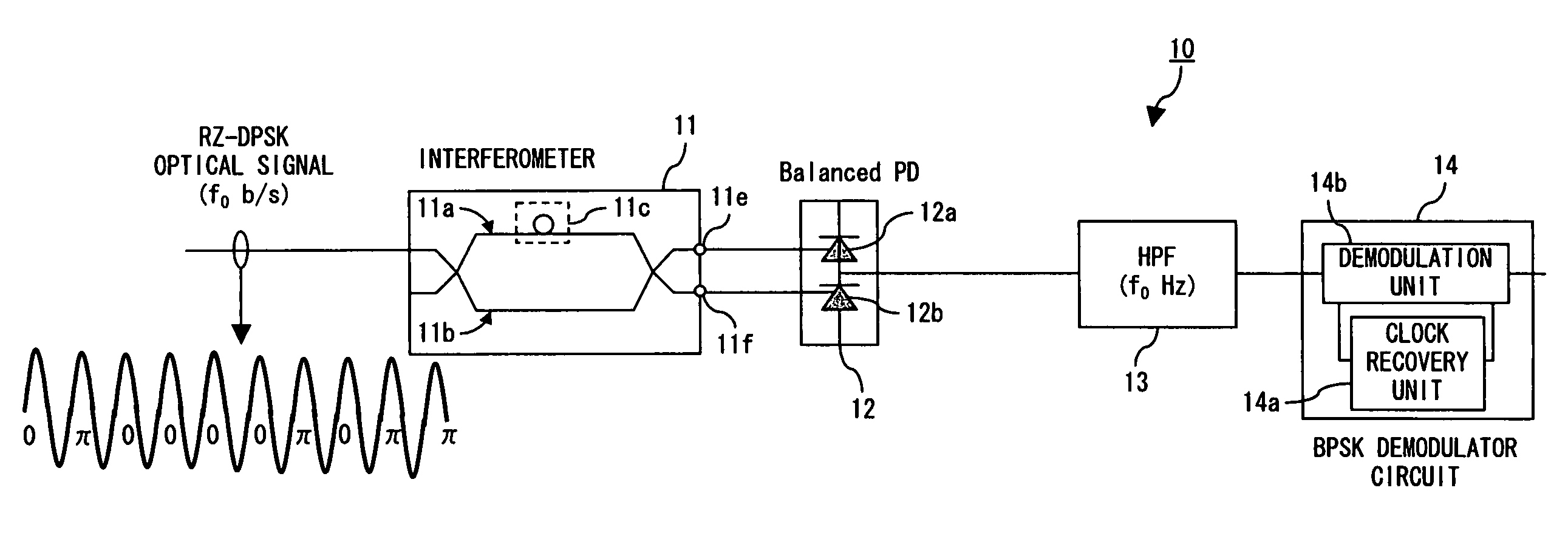
[0064]FIG. 11 is a diagram showing a configuration of an optical receiver circuit of the first embodiment. The interferometer 11, the balanced photodiode 12, the high-pass filter 13 and the BPSK demodulator circuit 14 can be the same as the above.

[0065]An amplifier 31 is provided between the balanced photodiode 12 and the high-pass filter 13, and amplifies the differential reception signal acquired by the balanced photodiode 12. By providing the amplifier 31, the receiver sensitivity is improved.

[0066]A low-pass filter 32 filters the differential reception signal amplified by the amplifier 31. The cut-off frequency of the low-pass filter 32 is about 70 percent of the data rate (f0) of the transmission data, for example. By providing the low-pass filter 32, the noise is removed and the waveform is improved.

[0067]A determination circuit 33 is a D flip-flop, for example, and determines the logical value of the output signal of the low-pass filter 32 at rising edge timing of a clock sig...

second embodiment

[0069]FIG. 12 is a diagram describing a configuration of an optical receiver circuit of the second embodiment. The interferometer 11, the balanced photodiode 12, the high-pass filter 13, the BPSK demodulator circuit 14, the amplifier 31, the low-pass filter 32 and the determination circuit 33 can be the same as explained above.

[0070]A variable delaying circuit 41 delays a clock signal provided from the BPSK demodulator circuit 14 to the determination circuit 33. The delay created by the variable delaying circuit 41 is adjusted by a control signal generated by a control circuit 43. An exclusive OR circuit 42 performs exclusive OR operation of data stream output from the BPSK demodulator circuit 14 and data stream output from the determination circuit 33. The control circuit 43 generates a control signal for adjusting the delay of the variable delaying circuit 41 based on the exclusive OR data.

[0071]In the optical receiver with the above configuration, when the phase of a clock signal...

third embodiment

[0073]FIG. 14 is a diagram showing a configuration of an optical receiver circuit of the third embodiment. The interferometer 11, the balanced photodiode 12, the high-pass filter 13, the BPSK demodulator circuit 14, the amplifier 31, the low-pass filter 32, the determination circuit 33, and the exclusive OR circuit 42 can be the same as explained above.

[0074]A limiter amplifier 51 amplifies the output signal of the low-pass filter 32 to a prescribed limit value, using a dynamically adjustable determination point (a threshold level). As the determination point changes, the waveform of the output signal of the limiter amplifier 51 also changes accordingly. The determination circuit 33 determines the logical value of the signal amplified by the limiter amplifier 51 using the clock signal provided from the BPSK demodulator circuit 14. A control circuit 52 controls the determination point of the limiter amplifier 51 based on the output of the exclusive OR circuit 42. At that time, when t...


PUM


Abstract

A received RZ-DPSK signal is guided to an interferometer. The interferometer comprises a 1-bit delaying element in an upper arm. A balanced photodiode converts a pair of optical signals output from the interferometer into electrical signal. A high-pass filter, which has a cut-off frequency equal or approximately equal to the symbol rate of transmission data, filters the signal output from the balanced photodiode. A BPSK demodulator circuit demodulates the output signal of the high-pass filter.

Description

BACKGROUND OF THE INVENTION[0001]1. Field of the Invention[0002]The present invention relates to an optical receiver circuit for receiving an RZ-DPSK optical signal and for demodulating it.[0003]2. Description of the Related Art[0004]As a technology for transmitting signals in an optical transmission system, phase modulation has been put to practical use widely. In the phase modulation, data is transmitted by shifting a phase of a carrier wave in accordance with data to be transmitted. In Binary Phase Shift Keying (BPSK) modulation, for example, “θ” and “θ+π” are assigned to data “0” and “1” in each bit, respectively. In Quaternary Phase Shift Keying (QPSK) modulation, “θ”, “θ+π / 2”, “θ+π” and “θ+3π / 2” are assigned to each symbol comprising 2-bit data, “00”, “01”, “11” and “10”, respectively. Here, “θ” is an arbitrary phase. A receiver apparatus can regenerate the transmitted data by detecting the phase of the received signal.[0005]When increasing transmission speed or distance of a ...

Claims


Application Information

Patent Timeline
Patent Type & Authority Patents(United States)
IPC IPC(8): H04B10/06H04B10/04H04B10/40H04B10/07H04B10/50H04B10/516H04B10/60H04B10/61H04B10/67H04B10/69
CPCH04B10/677
Inventor IKEUCHI, TADASHI
Owner FUJITSU LTD
Why Eureka
Try Eureka