Method of alignment of an optical module and an optical module using thereof

a technology of optical modules and alignment methods, applied in the direction of optical elements, instruments, semiconductor lasers, etc., can solve the problems of inapplicability, method defects, manufacturing methods as described above are not adapted,

Inactive Publication Date: 2009-11-03
HITACHI LTD
View PDF4 Cites 8 Cited by
  • Summary
  • Abstract
  • Description
  • Claims
  • Application Information

AI Technical Summary

Benefits of technology

[0014]The present invention has been made to solve the problems as described above, and an object of the present invention is to provide a method of alignment ensuring precise position adjustment between a surface emitting laser and a lens member during manufacture of an optical module, and an optical module manufactured by applying the method.
[0016]In an optical module in which a lens is used for optical coupling between a surface emitting laser and an optical fiber or an optical waveguide, even when a lens in the lens member and a surface emitting laser are away from each other, the lens and the surface emitting laser can precisely be coupled to each other optically.

Problems solved by technology

Especially it is not practical, from the view point of mass productivity and cost, to manufacture an engagement section for a board for a photonic device with high precision by machining.
Therefore, it can be understood that the manufacturing method as described above is not adapted to manufacture of a high speed optical module ensuring strong optical coupling currently required.
On the other hand, the method has the defects as described below.
With the structure based on the prior art, also a distance between the two marks is larger, so that it is impossible to align the photonic device and the lens with high positional precision.

Method used


Image

  • Method of alignment of an optical module and an optical module using thereof
  • Method of alignment of an optical module and an optical module using thereof
  • Method of alignment of an optical module and an optical module using thereof

Examples


first embodiment

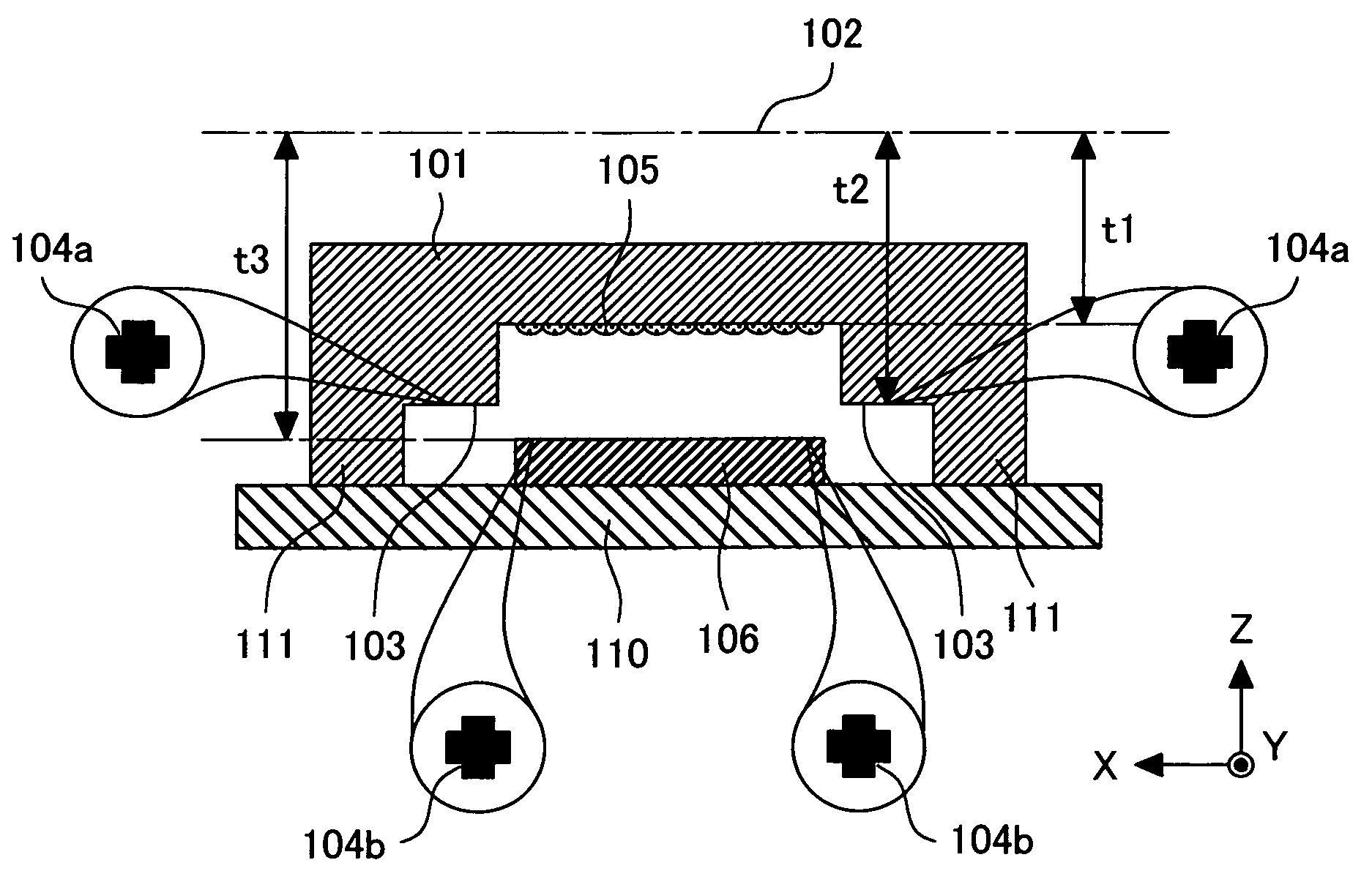
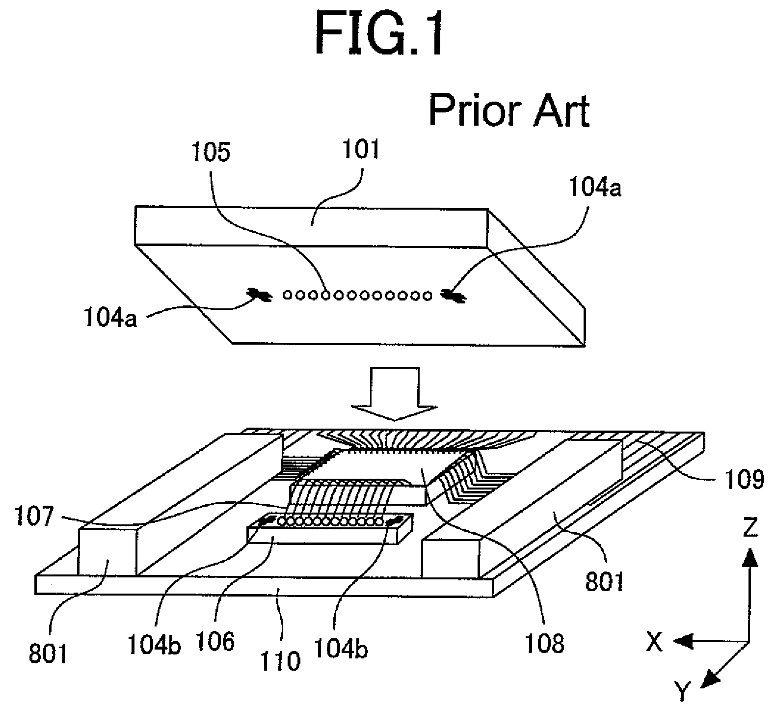
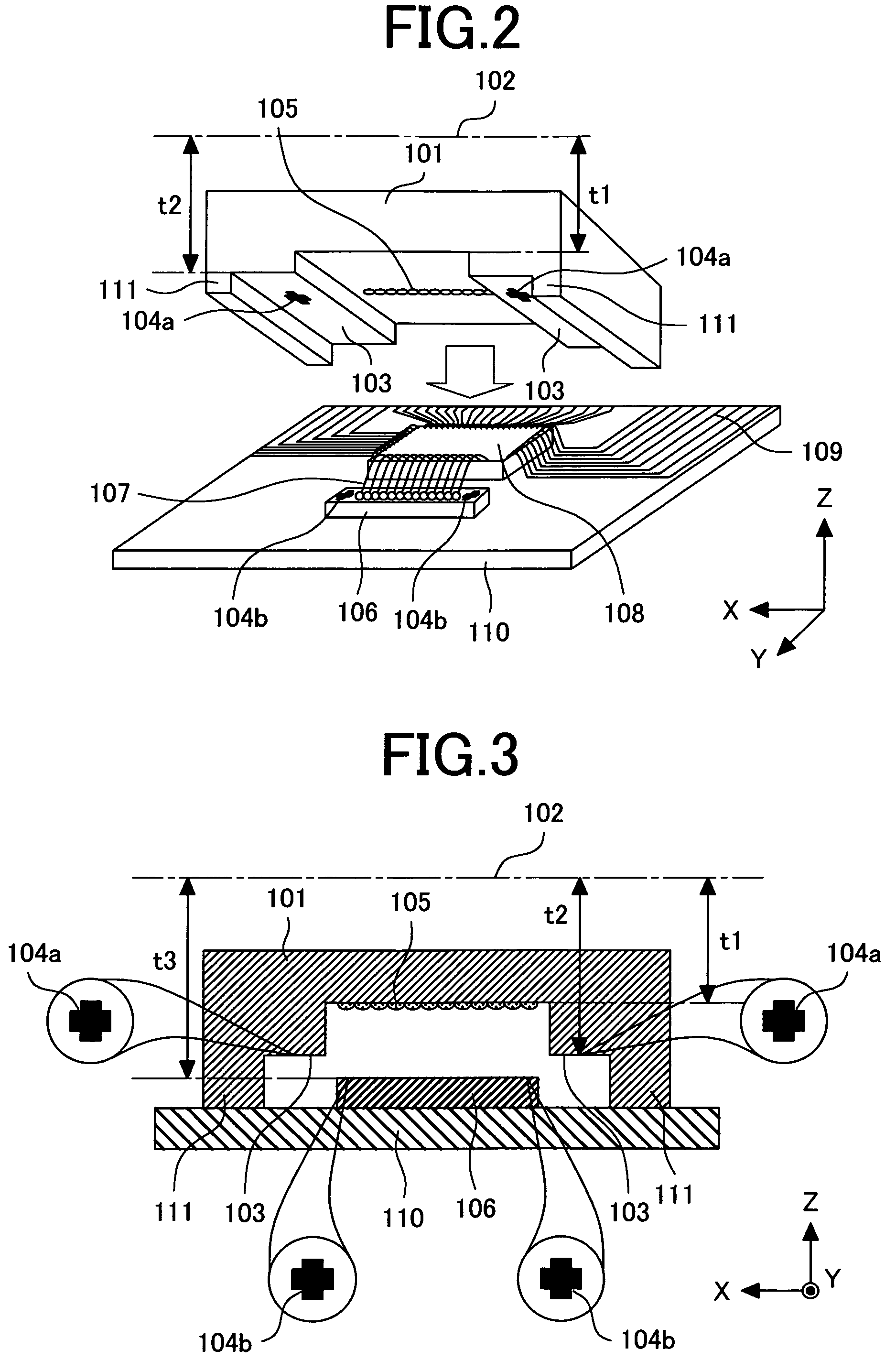
[0036]FIG. 2 is a view illustrating a case where position adjustment with alignment marks according to a first embodiment of the present invention is applied to an optical module. FIG. 3 is a cross-sectional view illustrating an optical module in which position adjustment with the alignment marks according to the first embodiment is applied, and the cross-section is taken at a position of a lens array 105. An IC 108 and a surface emitting laser 106 are mounted on a board 110 for a photonic device. An alignment mark 104b is provided on a top surface of the surface emitting laser 106. Wiring 107 is provided between the IC 108 and the surface emitting laser 106, and electric wiring 109 for connection to an external circuit is provided on the IC 108. A lens member 101 with the lens array 105 formed thereon is arranged at a position opposite to the surface emitting laser 106. In the first embodiment, a supporting member 111 is formed as a spacer at each of the two end portions in place o...

second embodiment

[0044]In the first embodiment, the alignment mark 104a is provided on the end face 103 of the protruding portion of the lens member 101 and also the alignment mark 104b is provided on the surface emitting laser 106. A second embodiment of the present invention uses the alignment mark 104b for the surface emitting laser 106.

[0045]FIG. 10A to FIG. 10C are plan views each illustrating a top surface of the surface emitting laser 106. FIG. 10A is a view corresponding to FIG. 5, and in FIG. 10A, light-emitting devices or light-receiving devices 1101 are shown in place of the lens array 105. FIG. 10A illustrates an example of the surface emitting laser 106 according to the first embodiment, and the alignment mark 104b is provided thereon.

[0046]FIG. 10B illustrates a case different from that shown in FIG. 10A, in which a line 120 surrounding the light-receiving devices 1101 and electrodes 401 is used in place of the alignment mark 104b described above. FIG. 10C illustrates an example in whi...

third embodiment

[0048]FIG. 11 is a cross-sectional view illustrating the configuration similar to that shown in FIG. 3, in which alignment marks 104b and 104a are provided on a surface of the board 110 for a photonic device and at an end of the end face 103 of a protruding portion of the lens member respectively. The alignment mark 104b is used to precisely mount the surface emitting laser 106 on the board 110 for a photonic device, and also functions as a reference for positioning the lens member 101. As a result, relative positions of the surface emitting laser 106 and the lens member 101 can be decided correctly.


PUM


Abstract

The present invention provides a method for high precision alignment of a surface emitting laser and a lens in an optical module in which optical coupling between a surface emitting laser and other optical devices such as an optical fiber is realized via lenses, and a structure for providing the method. A lens member 101, in which the lenses 105 are arrayed at a depth t1 from a reference plane 102 and an alignment mark is provided at a depth t2 (t1<t2) is prepared. Then alignment is performed for the lens 105 and the surface emitting laser 106 mounted on the board 110 for a photonic device.

Description

CLAIM OF PRIORITY[0001]The present application claims priority from Japanese Application JP 2005-266402 on Sep. 14, 2005, the content of which is hereby incorporated by reference into this application.FIELD OF THE INVENTION[0002]The present invention relates to a method of aligning a lens and an optical device in manufacture of an optical module for transmitting and receiving an optical signal and an optical module manufactured by applying the method.BACKGROUND OF THE INVENTION[0003]In association with rapid popularization of the Internet in recent years, a transfer capacity of a backbone optical network provided by a service provider has been becoming increasingly larger. Therefore, there is the strong need for development of a large capacity, low cost, and low power consumption optical module for connected in or between the devices in a facility where a large capacity router, a multiplex transmission device or the like are installed.[0004]There have been proposed various ideas for...

Claims


Application Information

Patent Timeline
Patent Type & Authority Patents(United States)
IPC IPC(8): G01B11/00
CPCG02B6/4204G02B6/4224H01S5/183H01S5/02288G02B6/4234H01L2224/49175H01L2224/48137H01S5/02253
Inventor BAN, TAKUMAMATSUOKA, YASUNOBUSHISHIKURA, MASATO
Owner HITACHI LTD
Why Eureka
Try Eureka