Sense-amplifier assist (SAA) with power-reduction technique

a technology of power reduction and amplifier assist, which is applied in the direction of digital storage, instruments, semiconductor devices, etc., can solve the problems of limiting the operating voltage of sram arrays, saa cannot be implemented, and sram may have a problem with meeting the voltage requirements of low-power embedded applications, so as to reduce the power of memory arrays, prevent leakage, and maintain read data timing

Inactive Publication Date: 2009-11-03
GLOBALFOUNDRIES INC
View PDF8 Cites 13 Cited by
  • Summary
  • Abstract
  • Description
  • Claims
  • Application Information

AI Technical Summary

Benefits of technology

[0022]Furthermore, the present invention limits the voltage level or amount of time that internal nodes NT, NC rises. Thus, the stability margin of the cell improves. Moreover, the present invention is implemented with a minimal area penalty (i.e., <1%).
[0026]Another embodiment of the present invention is a method for reducing power in a memory array comprising: (1) coupling sense-amplifier assist circuitry to each column of the memory array; (2) setting the sense-amplifier assist circuitry on each column during both READ and WRITE cycles; (3) masking the sense-amplifier assist circuitry coupled to half-selected columns; (4) discharging bit-lines of the memory array to ground on both half-selected columns and fully-selected columns; (5) discharging internal cell nodes of the memory array; (6) performing a full WRITE-back of READ data to cells of the memory array disturbed during the READ cycles; and (7) maintaining READ data timing between the half-selected columns and fully-selected columns. In addition, the memory device is preferably a static random access memory (SRAM).
[0027]Moreover, the method of the present invention preferably further comprises: pre-charging global bit-lines to VSS during READ cycles; reinforcing the discharge of data lines during READ cycles via feedback from global bit-lines and preventing leakage to unselected global bit-lines. In particular, reinforcing the discharge is done when device TGT or TGC is turned on to drive global bit-lines GBLT or GBLC high. This turns on device TWT or TWC to aid in the discharge of the data line DLT or DLC. Preventing leakage to unselected global bit-lines in unselected subarrays occurs when device TD is active (i.e., as SUBSEL is low). This prevents the discharge of DLC or DLT so that DLC / DLT are kept at their VDD pre-charge state.

Problems solved by technology

These conditions limit the operating voltage of SRAM arrays.
This mode of operation is a problem for the background art using SAA circuitry with SRAM architectures due to the power consumption penalty associated with these voltage transitions.
In some background art embedded applications, the additional power consumption that results from the above-discussed voltage transitions on the bit-lines is intolerable and thus, SAA cannot be implemented.
However, without SAA, the SRAM may have a problem with meeting the voltage requirements of low power embedded applications.
However, yet another problem exists with this background art circuit configuration.
This rise in voltage level on the internal nodes can disturb or distort the SRAM data.
Substantial variations in the voltage levels of the internal nodes NC, NT can eventually flip or disturb the state of the cell causing additional problems with this background art circuit configuration.
However, a problem with these short bit-line architectures is that they are not an effective means for improving stability in low-power technologies where the SRAM READ currents are very small.
Further, the SRAM array efficiency with short bit-line architectures is so poor that this method is often an unacceptable solution even in higher power embedded applications.

Method used


Image

  • Sense-amplifier assist (SAA) with power-reduction technique
  • Sense-amplifier assist (SAA) with power-reduction technique
  • Sense-amplifier assist (SAA) with power-reduction technique

Examples


Embodiment Construction

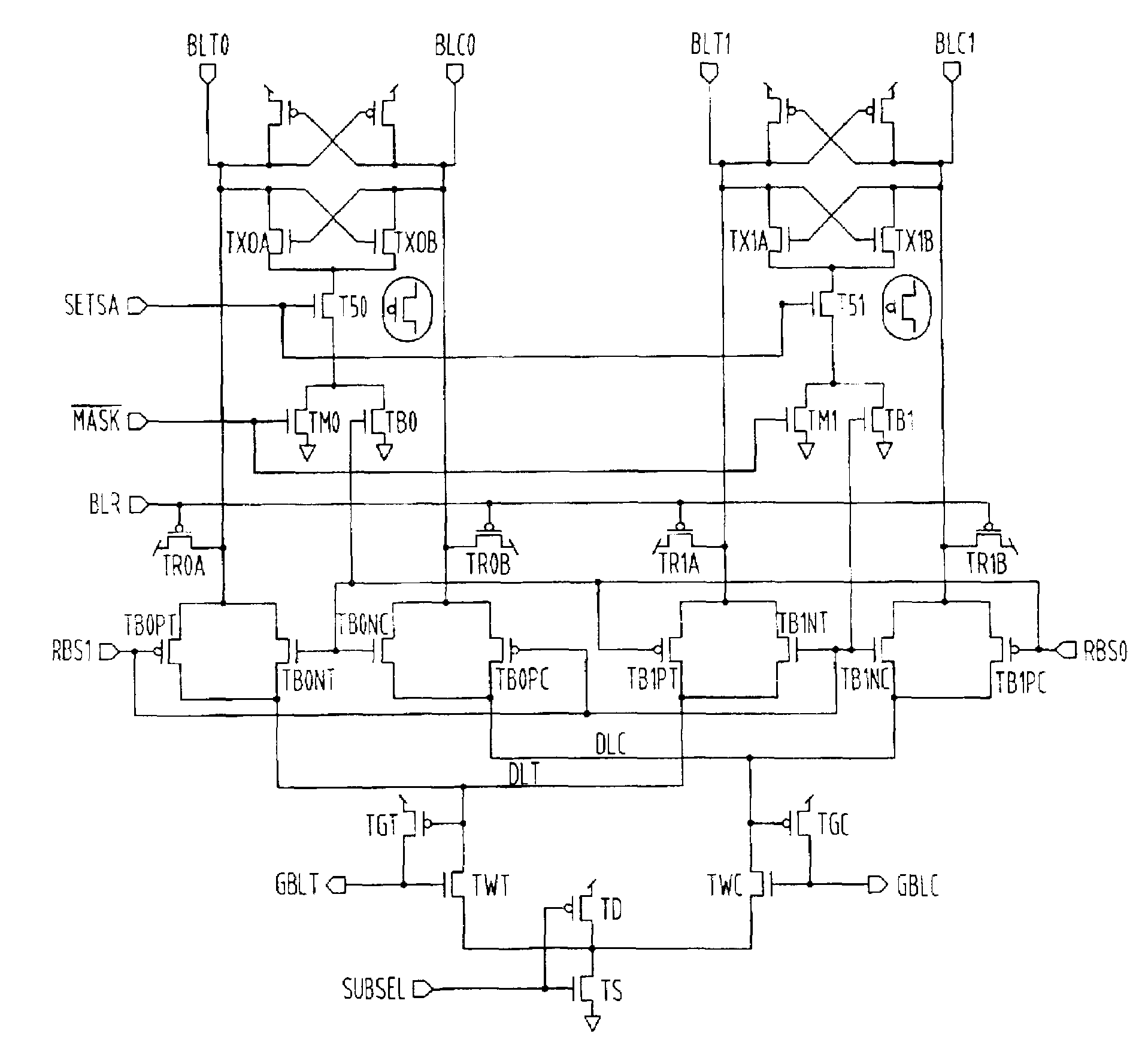
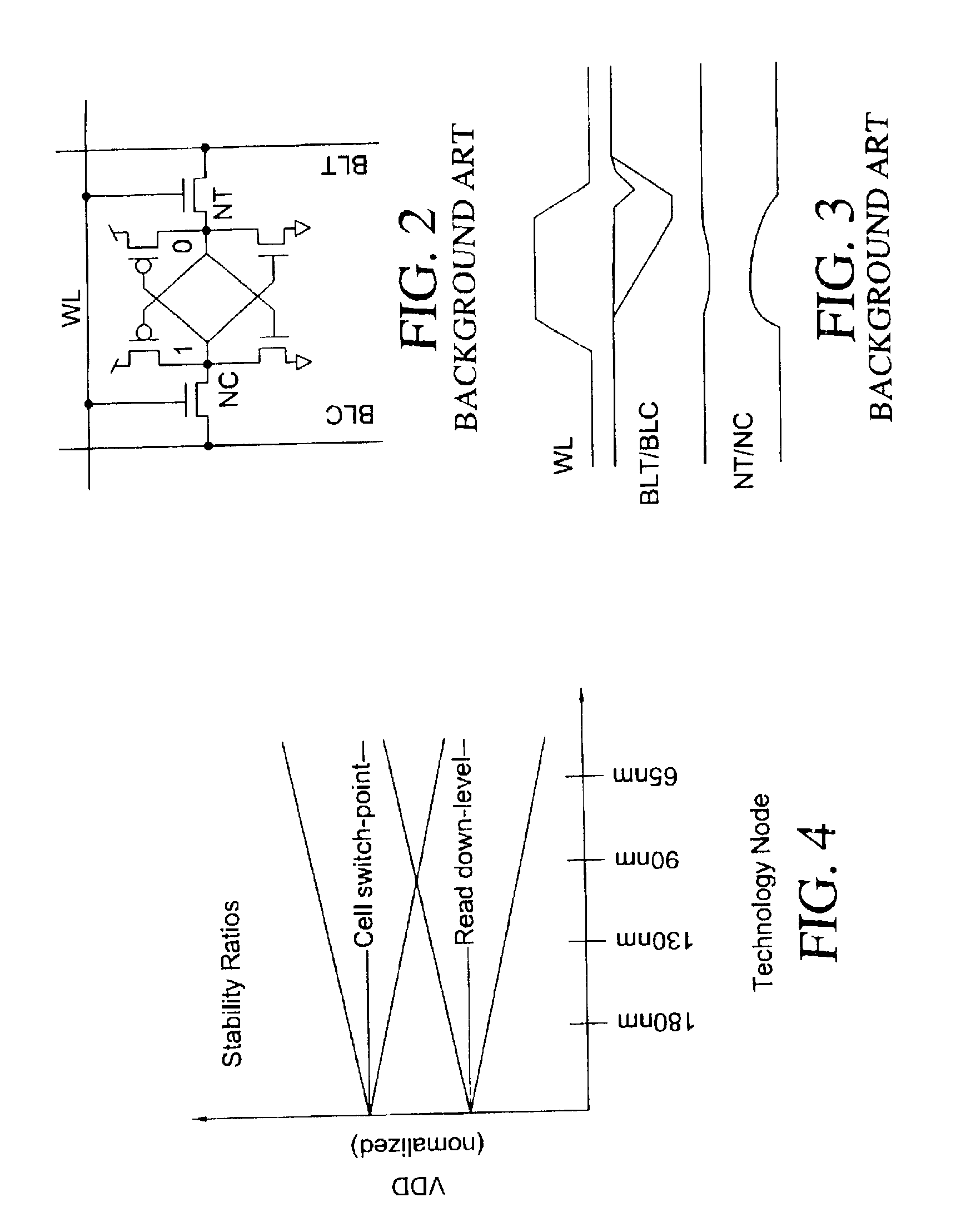
[0044]The present invention is an apparatus and method for improving the operating voltage range and stability margin of SRAM arrays. As semiconductor technology scales down to smaller feature sizes, SRAM cells are becoming more sensitive to lower operating voltages. For example, when a cell is read, the data in the SRAM cell can be disturbed or distorted.

[0045]FIG. 5 shows an exemplary block diagram of the SSA circuitry 500 of the present invention. In particular, FIG. 5 shows each subarray, bank or macro 506, 508, 510 of the SRAM apparatus has a mask-bit register 507, 511, 515. During functional tests, the subarrays, banks or macros are tested to a low-voltage corner by a BIST / TESTER 501. Subarrays with single-cell failures that go beyond redundancy repair capability have their mask registers set to ground (GND). Single cell failures induced in the field can be easily repaired using this circuitry. Setting the mask registers 507, 511, 515 to GND activates SAA circuitry 500 of the ...


PUM


Abstract

A design structure comprising an apparatus which reduces the power in memory devices in general and, in particular, static random access memory (SRAM) arrays featuring sense amplifier assist (SAA) circuitry. The design structure limits the implementation of the SAA circuitry to SRAM array blocks that do not meet the application voltage requirements.

Description

CROSS REFERENCES TO RELATED APPLICATIONS[0001]This Application is a continuation in part of U.S. application Ser. No. 11 / 424,072 filed Jun. 14, 2006, which is assigned to the present assignee.FIELD OF THE INVENTION[0002]This invention generally relates to a static random access memory (SRAM), and more particularly to a method for power reduction in such devices that utilize sense-amplifier assist (SAA) circuitry.BACKGROUND OF THE INVENTION[0003]A constant goal for the semiconductor industry is to continuously reduce the operating voltage and power required in semiconductor devices. The present invention is directed toward achieving this goal in SRAM arrays.[0004]SRAM or other conventional memory devices are typically included in electronic systems for data storage. These memory devices store data in arrays of memory cells. Each cell conventionally stores a single bit of data (either a “1” or a “0”) and can be individually accessed or addressed. Data is output from a memory cell duri...

Claims


Application Information

Patent Timeline
Patent Type & Authority Patents(United States)
IPC IPC(8): G11C7/06G11C8/00H01L29/00
CPCG11C7/06G11C7/12G11C29/08G11C11/419G11C11/41G11C7/02
Inventor BRACERAS, GEORGE MARIAPILO, HAROLDTOWLER, FRED JOHN
Owner GLOBALFOUNDRIES INC
Why Eureka
Try Eureka