
Semiconductor integrated circuit with delay test circuit, and method for testing semiconductor integrated circuit

a technology of semiconductor integrated circuit and test circuit, which is applied in the direction of instruments, measurement devices, computing, etc., can solve the problems of inability to carry out at-speed delay test, circuit may be present, and inability to detect the delay,

Active Publication Date: 2009-11-03
RENESAS ELECTRONICS CORP
View PDF10 Cites 42 Cited by
  • Summary
  • Abstract
  • Description
  • Claims
  • Application Information

AI Technical Summary

Benefits of technology

This solution enables practical at-speed delay testing of multi-cycle and inter-domain paths by controlling clock pulse generation within the semiconductor integrated circuit, reducing data processing needs and eliminating impractical design restrictions, thus improving test efficiency and feasibility.

Problems solved by technology

This is because a fault that inappropriate delay is caused in the semiconductor integrated circuit may be present in the circuit despite a logically correct circuit configuration.
It is a restriction on an operating rate of an LSI tester that makes it difficult to carry out the at-speed delay test.
However, the use of the LSI tester having the high operating rate pushes up a test cost and is disadvantageous against a manufacturing cost of the semiconductor integrated circuit.
The second conventional example points out that a difference in delay between the clock trees is an obstacle to the at-speed delay test to an inter-domain path, which is a path for transmitting a signal from a flip-flop belonging to one clock domain to a flip-flop belonging to another clock domain.
However, the technique disclosed in the first conventional example is disadvantageous in testability of a multi-cycle path.
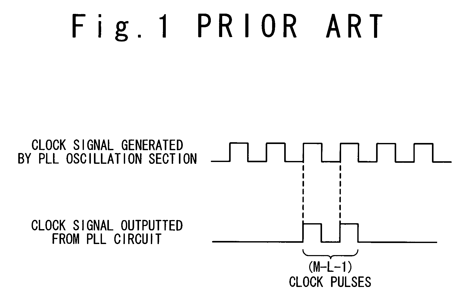
In the semiconductor integrated circuit with the PLL circuit which can generate only continuous clock pulses, as disclosed in the first conventional example, the presence of this multi-cycle path is quite inconvenient for the at-speed delay test using the ATPG tool.
As could be understood, the use of the multi-cycle path disadvantageously increases a data processing amount necessary for the ATPG tool to generate the test patterns, and necessitates a large capacity of memory to store internal states of the semiconductor integrated circuit, such as the values of scan flip-flops in each clock period.
For the semiconductor integrated circuit as large as over ten million gates in scale, increases in the necessary data processing amount and memory capacity are too serious to be accepted economically.
Therefore, when the semiconductor integrated circuit includes the PLL circuit that can generate only continuous clock pulses, it is eventually impossible to carry out the at-speed delay test to the multi-cycle path.
Meanwhile, in the second conventional example, an unpractical design restriction is sometimes imposed on the semiconductor integrated circuit to adjust delays of the clock trees.
Therefore, in order to compensate the above delay difference, it would be necessary to provide impractically large number of delay gates between the PLL circuit and the input of the clock tree for adjusting the delays of the clock trees by the delay gates.
This indicates that it is impractical to carry out the at-speed delay test to the inter-domain path by adjusting the delay difference between the clock trees by using the delay gates.
As could be understood from the above, no practical techniques for carrying out the at-speed delay test to the multi-cycle path or the inter-domain path are present.

Method used


Image

  • Semiconductor integrated circuit with delay test circuit, and method for testing semiconductor integrated circuit
  • Semiconductor integrated circuit with delay test circuit, and method for testing semiconductor integrated circuit
  • Semiconductor integrated circuit with delay test circuit, and method for testing semiconductor integrated circuit

Examples


first modification

[First Modification]

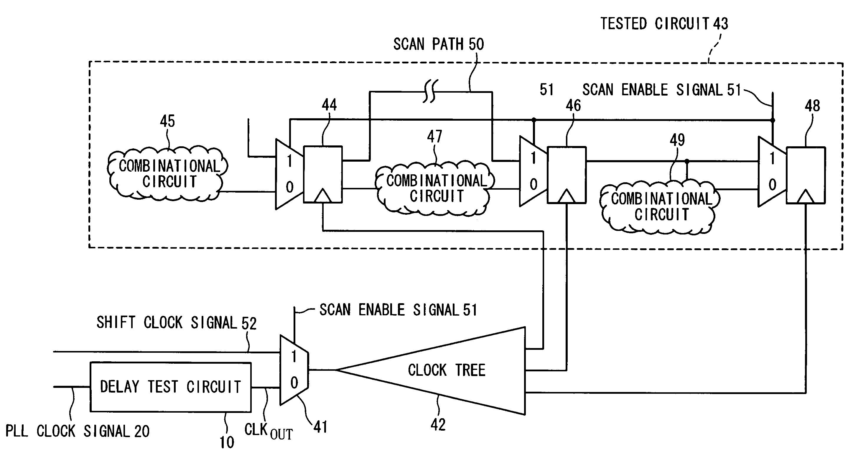
[0099]In the semiconductor integrated circuit shown in FIG. 11, if the difference in delay time between the first clock tree 62A and the second clock tree 62B is great, it is necessary to increase the difference between output timings of clock pulses outputted from the delay test circuits 10A and 10B. An upper limit of the difference between the output timings of the clock pulses depends on the number of bits of the clock waveform setting data 14 settable to the delay test circuits 10A and 10B. For instance, if the number of bits of the clock waveform setting data 14 is four, the difference in delay time between the first clock tree 62A and the second clock tree 62B is allowed up to three clock periods of the test reference clock signal 74.

[0100]The simplest method for increasing the difference between output timings at which the delay tests 10A and 10B output the clock pulses is to increase the number of bits of the clock waveform setting data 14 supplied to at ...

second modification

[Second Modification]

[0107]As evident from the operations of the delay test circuits 10 described above, in the semiconductor integrated circuit shown in FIG. 11, the timings at which the delay test circuits 10A and 10B output the clock pulses are adjusted in units of clock periods of the test reference clock signal 74. However, the difference in delay between the first clock tree 62A and the second clock tree 62B is not always in units of clock periods. It is, therefore, preferable to be able to adjust the timings at which the delay test circuits 10A and 10B output the clock pulses more minutely.

[0108]FIG. 15 is a circuit diagram of a configuration of a semiconductor integrated circuit for making it possible to adjust the timings at which the delay test circuits 10A and 10B output the clock pulses more minutely. In the configuration of FIG. 15, one of the input PLL clock signal 20A supplied to the delay test circuit 10A and the input PLL clock signal 20B supplied to the delay test ...


PUM


Abstract

A semiconductor integrated circuit includes an input side flip-flop; a combinational circuit having an input connected with the input side flip-flop; an output side flip-flop connected with an output of the combinational circuit; and a delay test circuit. The delay test circuit generates output clock pulses by removing an optional one from equal to or more than 3 continuing clock pulses of an input clock signal, and supplies the output clock pulse to the input side flip-flop and the output side flip-flop.

Description

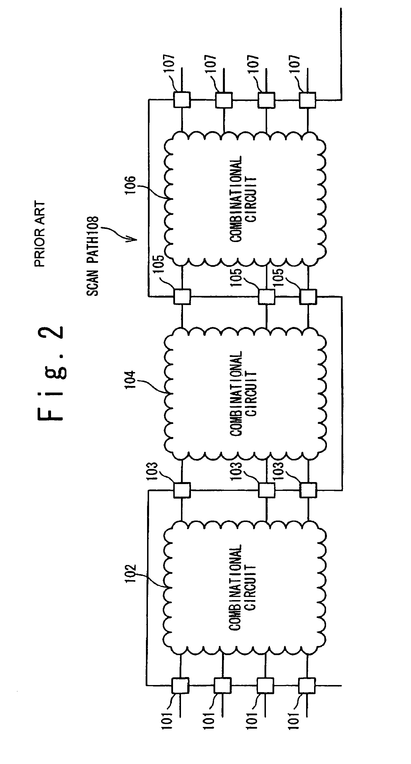
BACKGROUND OF THE INVENTION[0001]1. Field of the Invention[0002]The present invention relates to a semiconductor integrated circuit with a delay test circuit, and a method for testing the semiconductor integrated circuit. More specifically, the present invention relates to a technique for facilitating a test of a semiconductor integrated circuit using a scan path.[0003]2. Description of the Related Art[0004]One of the most widely used techniques for facilitating a test of a semiconductor integrated circuit is a scan design technique for incorporating scan paths into the semiconductor integrated circuit. Specifically, the flip-flops of a core logic are connected in series to form the scan path, and a selector is additionally provided for a data input of each of flip-flops. The flip-flops are often referred to as “scan flip-flops”. This scan path functions as a very large scale of shift register. At the time of testing the core logic, a data is directly written into or read from the s...

Claims


Application Information

Patent Timeline
Patent Type & Authority Patents(United States)
IPC IPC(8): G01R31/28
CPCG01R31/31858
Inventor ASAKA, TOSHIHARU
Owner RENESAS ELECTRONICS CORP
Learn More