Solid-state image device and camera including solid-state image device for selective outputs

a solid-state image and image device technology, applied in the direction of television systems, instruments, color signal processing circuits, etc., can solve the problems of more severe problems than maintaining known battery longevity, new technological problems, and inability to achieve the effect of reducing dark current non-uniformity and excellent quality

Inactive Publication Date: 2009-11-17
CANON KK
View PDF5 Cites 5 Cited by
  • Summary
  • Abstract
  • Description
  • Claims
  • Application Information

AI Technical Summary

Benefits of technology

[0017]The present invention provides a solid-state image device that has a structure in which an external amplifier is disposed near the solid-state image device and that is capable of reducing dark current nonuniformity caused by an internal amplifier of the solid-state image device and the external amplifier disposed near the solid-state image device and acquiring images of an excellent quality.
[0018]In order to suppress generation of dark current nonuniformity, an output unit dedicated to long-time accumulation, which requires only a small current consumption and suppresses impact ionization, is provided in addition to an output amplifier disposed inside the solid-state image device. In addition, with a structure in which the external amplifier is disposed in close vicinity to the solid-state image device, the power source of the external amplifier is turned off during the accumulation time in order to reduce dark current nonuniformity. The output unit configured to output a voltage dedicated to long-time accumulation is provided so that the external amplifier does not exceed the rated voltage.
[0021]Accordingly, the current consumption of the entire solid-state image device is reduced, generation of dark current nonuniformity is suppressed, and the rated voltage of the external amplifier is not exceeded.

Problems solved by technology

However, due to the recent advancement of technologies, the signal-to-noise ratio of signal outputs have been improved, and new technological problems have occurred.
Thus, a problem in which dark current nonuniformity occurs on a screen, which is unique to solid-state image devices, occurs.
This problem is more severe than maintaining known battery longevity.
This is because an extremely long time, such as several minutes or several tens of minutes, is required for accumulation.
In addition, for the internal amplifier, depending on the operation voltage of a transistor used, dark current nonuniformity occurs even when a current of several tens of microamperes flows.
In other words, only reducing currents, such as simply turning off a constant-current source, cannot prevent nonuniformity.
This problem cannot be handled by known ideas.
This causes the impact ionization phenomenon, and thus increasing the dark current nonuniformity.

Method used


Image

  • Solid-state image device and camera including solid-state image device for selective outputs
  • Solid-state image device and camera including solid-state image device for selective outputs
  • Solid-state image device and camera including solid-state image device for selective outputs

Examples


first embodiment

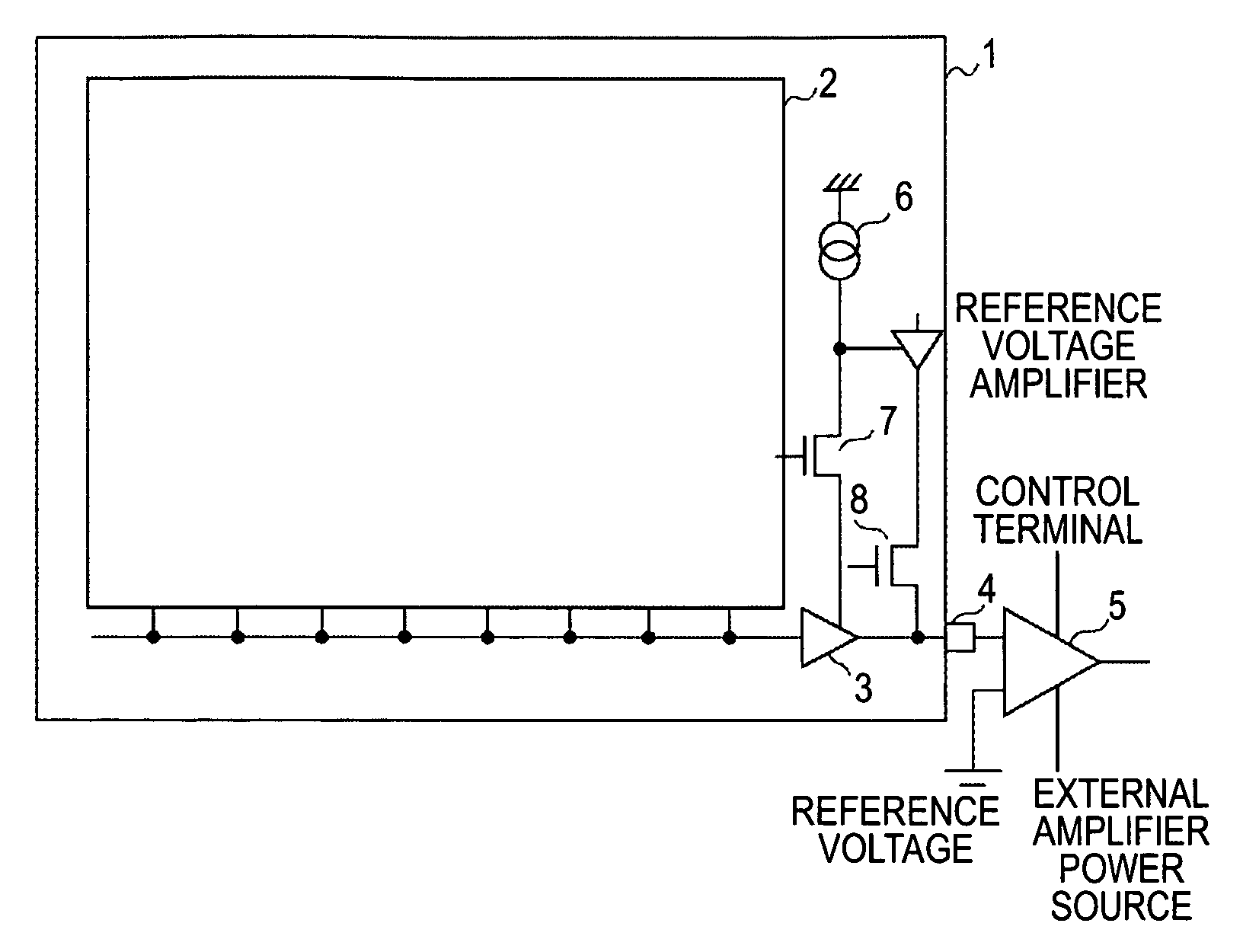
[0040]FIG. 1 is a schematic diagram schematically showing a solid-state image device according to a first embodiment of the present invention.

[0041]Reference numeral 1 denotes the entire solid-state image device. Pixels each including a photoelectric converter are arranged two-dimensionally in a pixel area 2. An output amplifier 3 outputs signals of the pixels. An external amplifier (provided with a control terminal) 5 is disposed near an output terminal 4. Reference numeral 6 denotes a current source of the output amplifier 3. A power-save switch 7 reduces the current consumption of the output amplifier 3. Reference numeral 8 denotes an output selection switch. These units are arranged as shown in FIG. 1.

[0042]A structure in which the external amplifier 5 is added to the solid-state image device 1 can also be referred to as a solid-state image device in terms of functionality. This is also applied to the embodiments described below.

[0043]In the first embodiment, during an accumulat...

second embodiment

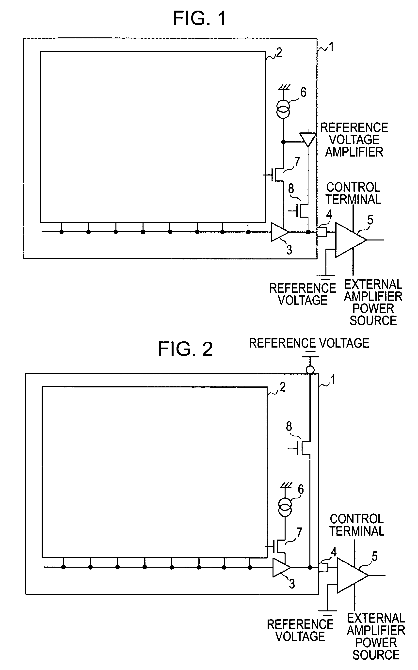
[0048]FIG. 2 is a schematic diagram schematically showing a solid-state image device according to a second embodiment of the present invention.

[0049]Reference numeral 1 denotes the entire solid-state image device. Pixels each including a photoelectric converter are arranged two-dimensionally in a pixel area 2. An output amplifier 3 outputs signals of the pixels. An external amplifier (provided with a control terminal) 5 is disposed near an output terminal 4. Reference numeral 6 denotes a current source of the output amplifier 3. A power-save switch 7 reduces the current consumption of the output amplifier 3. Reference numeral 8 denotes an output selection switch.

[0050]In the second embodiment, during an accumulation time, the current consumption of the output amplifier 3 is reduced using the power-save switch 7, and an increase in the dark current of a photoelectric converter located near the output amplifier 3 is thus suppressed. In addition, in order to reduce the current consumpt...

third embodiment

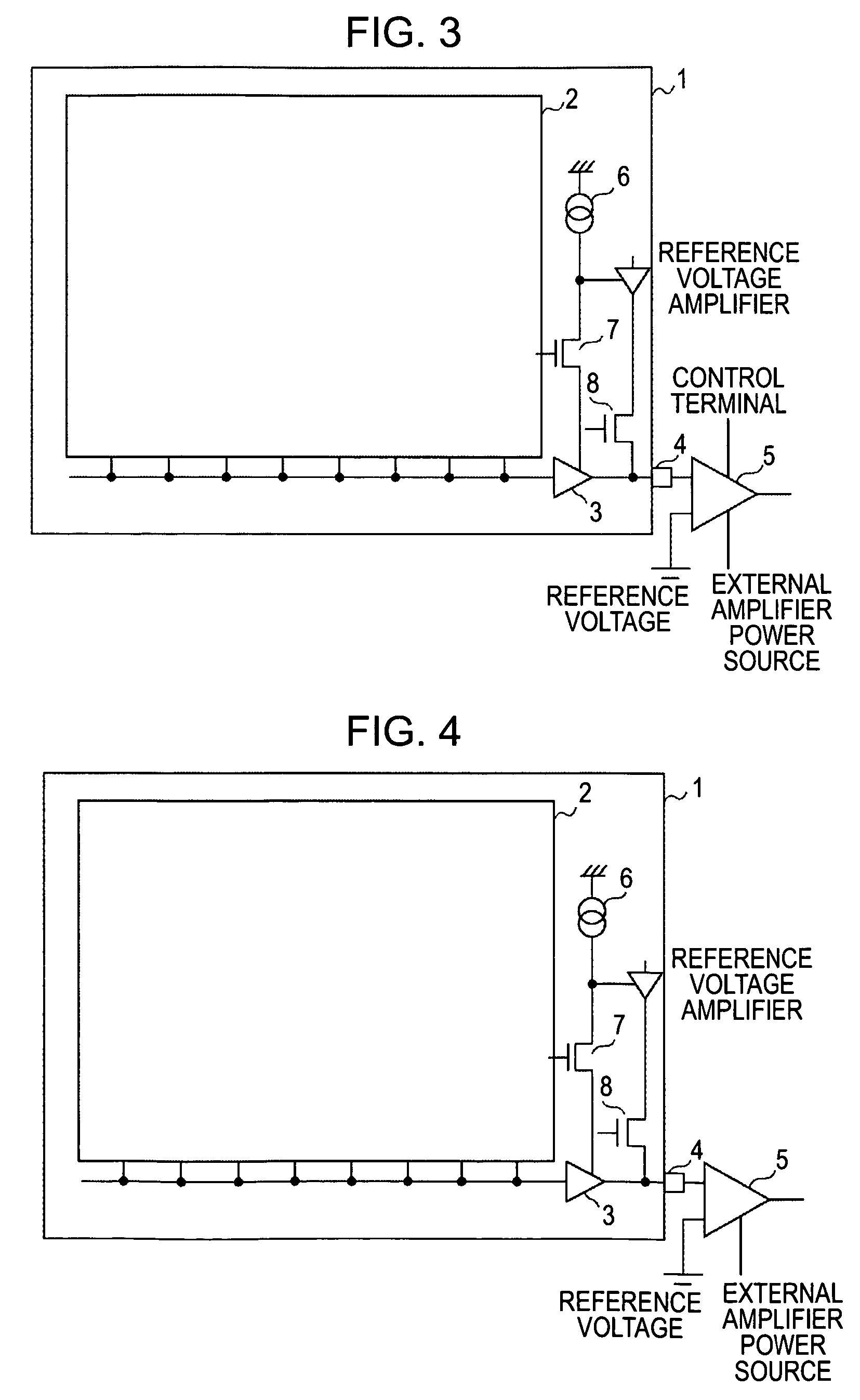
[0055]FIG. 3 is a schematic diagram schematically showing a solid-state image device according to a third embodiment of the present invention.

[0056]Reference numeral 1 denotes the entire solid-state image device. Pixels each including a photoelectric converter are arranged two-dimensionally in a pixel area 2. An output amplifier 3 outputs signals of the pixels. An external amplifier (provided with a control terminal) 5 is disposed near an output terminal 4. Reference numeral 6 denotes a current source of the output amplifier 3. A power-save switch 7 reduces the current consumption of the output amplifier 3. Reference numeral 8 denotes an output selection switch. These units are arranged as shown in FIG. 3.

[0057]In the third embodiment, during an accumulation time, the current consumption of the output amplifier 3 is reduced using the power-save switch 7, and an increase in the dark current of a photoelectric converter located near the output amplifier 3 is thus suppressed. In additi...


PUM


Abstract

A solid-state image device including pixels arranged two-dimensionally, the pixels each including a photoelectric converter for converting incident light into an electric signal, is provided. The solid-state image device includes an output amplifier configured to amplify a photoelectric conversion output from each of the pixels, and a reference voltage amplifier configured to output a reference voltage. The solid-state image device selectively outputs the photoelectric conversion output and the reference voltage.

Description

BACKGROUND OF THE INVENTION[0001]1. Field of the Invention[0002]The present invention relates to solid-state image devices including a plurality of photoelectric converters for converting incident light into electric signals.[0003]2. Description of the Related Art[0004]In image pickup apparatuses, such as digital cameras including a solid-state image device, in order to make signal outputs of the solid-state image device more tolerant to disturbance noise, an external amplifier is disposed in close vicinity to the solid-state image device and amplifies the outputs. This structure will be described with reference to FIG. 11. Reference numeral 1 denotes a solid-state image device. Pixels each including a photoelectric converter are arranged two-dimensionally in a pixel area 2. An output amplifier 3 outputs signals of the pixels. An external amplifier 5 is disposed near an output terminal 4. Reference numeral 6 denotes a current source of the output amplifier 3. A power-save switch 7 s...

Claims


Application Information

Patent Timeline
Patent Type & Authority Patents(United States)
IPC IPC(8): H04N9/64G06F3/041H03F3/00H04N5/335H04N5/353H04N5/361H04N5/378H04N101/00
CPCH04N5/361H04N5/378H04N5/3698H04N25/63H04N25/709H04N25/75
Inventor SAKAI, SEIICHIROUKOIZUMI, TORU
Owner CANON KK
Why Eureka
Try Eureka