Method and apparatus for high resolution ZQ calibration

a high-resolution zq and calibration method technology, applied in pulse generators, pulse techniques, instruments, etc., can solve the problems of impedance mismatch, external noise can affect the reflection characteristics of output signals, external noise increases,

Active Publication Date: 2009-12-01
MICRON TECH INC
View PDF14 Cites 18 Cited by
  • Summary
  • Abstract
  • Description
  • Claims
  • Application Information

AI Technical Summary

Problems solved by technology

However, as the signal swing width of a transmitted signal decreases, external noise increases.
External noise can affect the reflection characteristics of an output signal if there is an impedance mismatch at an interface.
Impedance mismatches are caused by external noise or by noise on a power supply voltage, temperature and process variations, among others.
If an impedance mismatch arises, the transmission speed of the data decreases, and the data from a semiconductor device may become distorted.
Thus, in a case where a semiconductor device receives distorted data, problems can be caused by setup / hold failures or errors in reading received data.
Because the calibration of VZQN is performed after calibration of VZQP, the voltage VZQN may have a two step error.
A two step error is a substantial error, particularly for the fast corner.

Method used


Image

  • Method and apparatus for high resolution ZQ calibration
  • Method and apparatus for high resolution ZQ calibration
  • Method and apparatus for high resolution ZQ calibration

Examples


Embodiment Construction

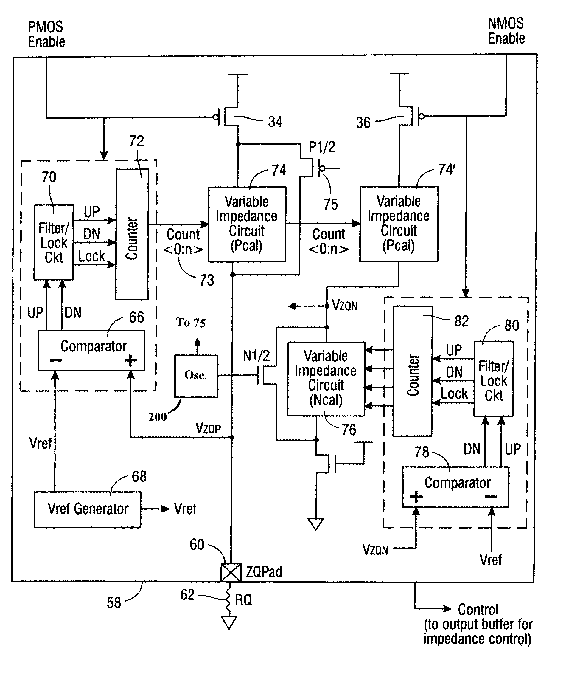
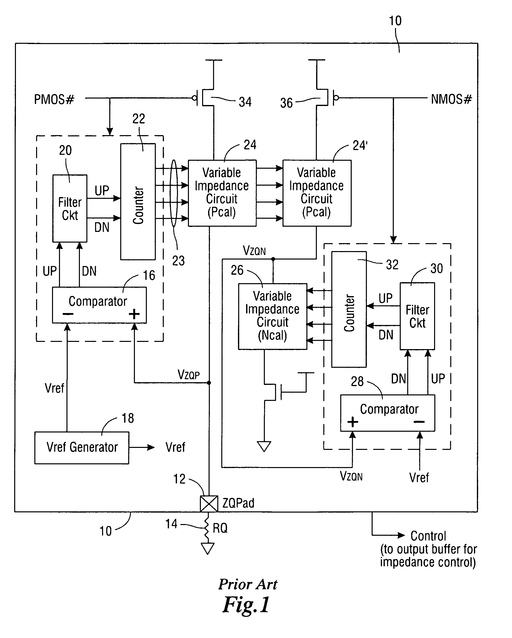
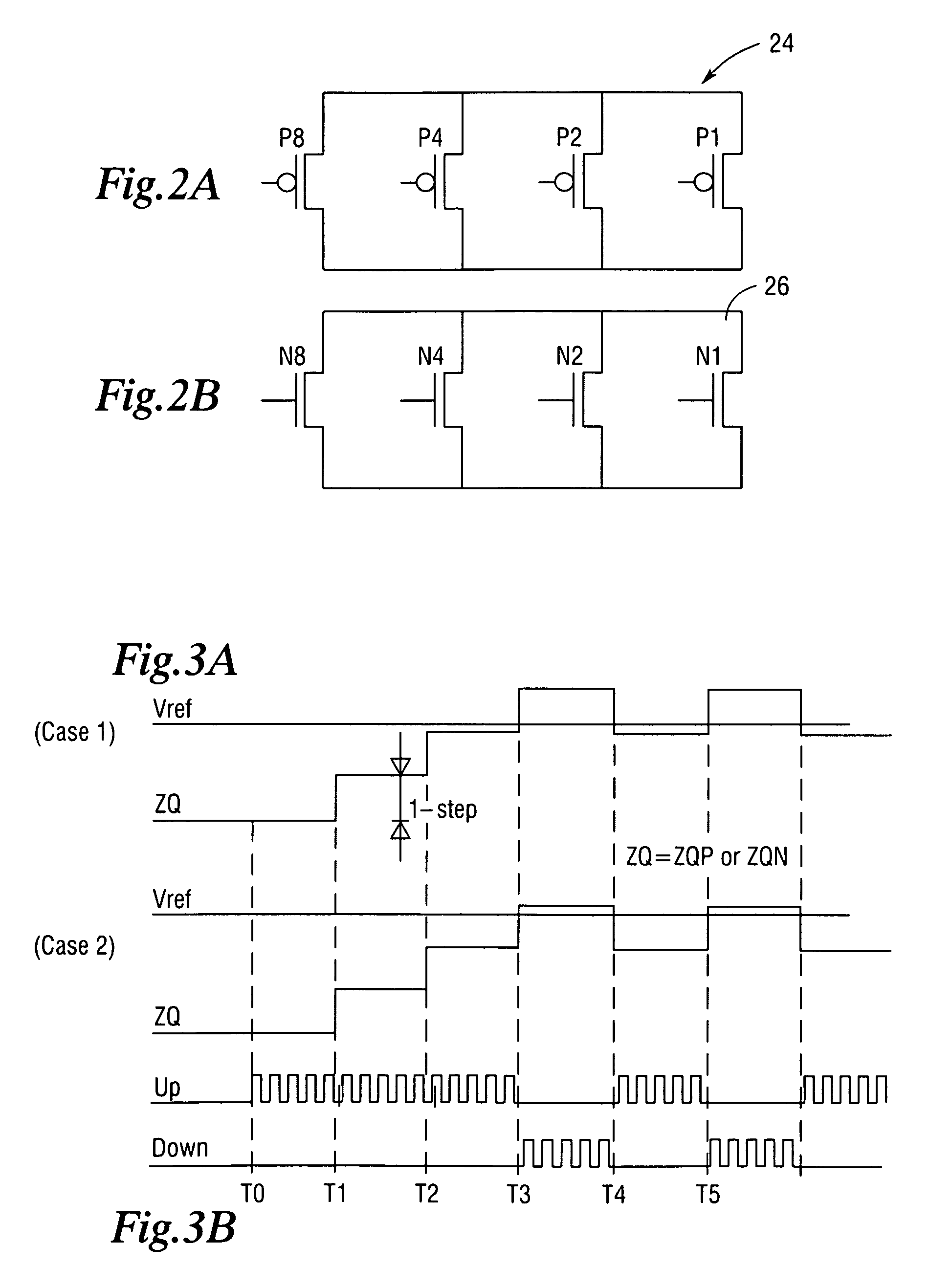
[0030]FIG. 4 is a simplified block diagram illustrating a memory chip or memory device 40. The memory chip 40 may be part of a DIMM (dual in-line memory module) or a PCB (printed circuit board) containing many such memory chips (not shown in FIG. 4). The memory chip 40 may include a plurality of pins or ball contacts 42 located outside of chip 40 for electrically connecting the chip 40 to other system devices. Some of those pins 42 may constitute memory address pins or address bus 44, data (DQ) pins or data bus 46, and control pins or control bus 48. It is evident that each of the reference numerals 44, 46, 48 designates more than one pin in the corresponding bus. Further, it is understood that the diagram in FIG. 4 is for illustration only. That is, the pin arrangement or configuration in a typical memory chip may not be in the form shown in FIG. 4.

[0031]A processor or memory controller (not shown) may communicate with the chip 40 and perform memory read / write operations. The proce...


PUM


Abstract

A method is disclosed for controlling an output impedance of an electronic device of the type having an impedance control terminal to which an external load is to be connected such that a predetermined value of the voltage at the impedance control terminal controls the output impedance of the device. The method is comprised of comparing a reference voltage to a voltage at the impedance control terminal. A variable count signal representing a count value is produced in response to the comparing. The impedance of a variable impedance circuit is varied in response to the count signal, wherein the impedance of the variable impedance circuit controls the voltage at the impedance control terminal. A device connected in parallel with the variable impedance circuit is periodically operated to change (increase / decrease) the impedance of the variable impedance circuit. An apparatus for performing the method is also disclosed. Because of the rules governing abstracts, this abstract should not be used to construe the claims.

Description

BACKGROUND OF THE INVENTION[0001]The present invention is directed generally to solid state devices and, more particularly, to such devices having a ZQ pad or terminal which may be used to control the output impedance of the device.[0002]Semiconductor devices such as microcomputers, memories, gate arrays, among others, include input / output pins and an output circuit for transmitting data to other devices, via a bus, transmission lines formed on a board, and the like. A circuit within the semiconductor device that is responsible for transmitting data includes, for example, output buffers and drivers. For there to be optimum transmission, the impedance of the transmitting device should be matched to the impedance of the transmission network and receiving device.[0003]As operational speeds of electronic devices increase, the swing of transmitted signals decreases. However, as the signal swing width of a transmitted signal decreases, external noise increases. External noise can affect t...

Claims


Application Information

Patent Timeline
Patent Type & Authority Patents(United States)
IPC IPC(8): H03K17/16G11C7/10H03K19/003
CPCH04L25/0278H03K19/0005
Inventor KIM, KANG YONG
Owner MICRON TECH INC
Why Eureka
Try Eureka