Common-mode bandwidth reduction circuit and method for differential applications

a common-mode bandwidth and reduction circuit technology, applied in the direction of dc-amplifiers with dc-coupled stages, dc-amplifiers with semiconductor devices/discharge tubes, differential amplifiers, etc., can solve the problems of severe differential amplifier driver circuit problems, differential amplifier driver circuits susceptible to common-mode instability, individual amplifiers and hence differential amplifier driver circuits that are composed thereof, etc., to avoid instability in response and achieve higher full power bandwidth

Active Publication Date: 2009-12-01
TEXAS INSTR INC
View PDF9 Cites 0 Cited by
  • Summary
  • Abstract
  • Description
  • Claims
  • Application Information

AI Technical Summary

Benefits of technology

[0016]It is an object of the invention to provide a differential amplifier driver circuit which avoids instability in response to both differential input signals and common-mode input signals and which also has higher full power bandwidth than the closest prior art.
[0017]It is another object of the invention to provide a differential amplifier driver circuit which avoids instability in response to both differential input signals and common-mode input signals and which dissipates less power at high frequencies than the closest prior art.

Problems solved by technology

Consequently, the individual amplifiers and hence the differential amplifier driver circuits amplifiers composed thereof tend to be unstable if operated at lower gains, and particularly at a gain of unity.
This represents a severe problem for the differential amplifier driver circuits when used in DSL applications.
Because of this, the differential amplifier driver circuit is susceptible to common mode instability.
However, as a matter of actual circuit implementation, adding an inverting amplifier to each amplifier block is not practical.
This places an undesirable burden on the signal current mirrors which increases with frequency and amplitude.
In fact, depending on the magnitude of the charging currents and discharging currents, there is a significant likelihood of high internal AC power dissipation and the possibility of inadequate full power bandwidth of circuits implementing this compensation method.
However, when the amplification is common mode amplification, the burden of charging and discharging capacitors 514 and 516 (and also capacitors 564 and 566) actually falls entirely on the current mirror output transistors, necessitating the use of substantially larger transistor geometries than would normally be used.
The above mentioned over-sizing of transistors tends to degrade / distort large signal circuit performance of the amplifier.
This, as well as the high charge / discharge current flowing in the complementary current mirror, limits large signal bandwidth, and also results in substantial additional power dissipation.
Also, if transistors 503, 504, 553, and 554 are not made sufficiently large, they will have difficulty supplying the charging currents and discharging currents, and therefore those transistors will have a tendency to saturate at high signal levels.
This causes the large signal frequency response of the differential amplifier driver circuit in U.S. Pat. No. 6,867,649 to deteriorate rapidly as the signal level increases.
A major disadvantage of the foregoing circuit is that the large common mode compensation capacitors must be complementarily charged and discharged for differential mode signals.
Although this method functions very well for small signals at moderate frequencies, it suffers from high internal power dissipation as the frequency is increased and it has limited large signal bandwidth capability.

Method used


Image

  • Common-mode bandwidth reduction circuit and method for differential applications
  • Common-mode bandwidth reduction circuit and method for differential applications
  • Common-mode bandwidth reduction circuit and method for differential applications

Examples


Embodiment Construction

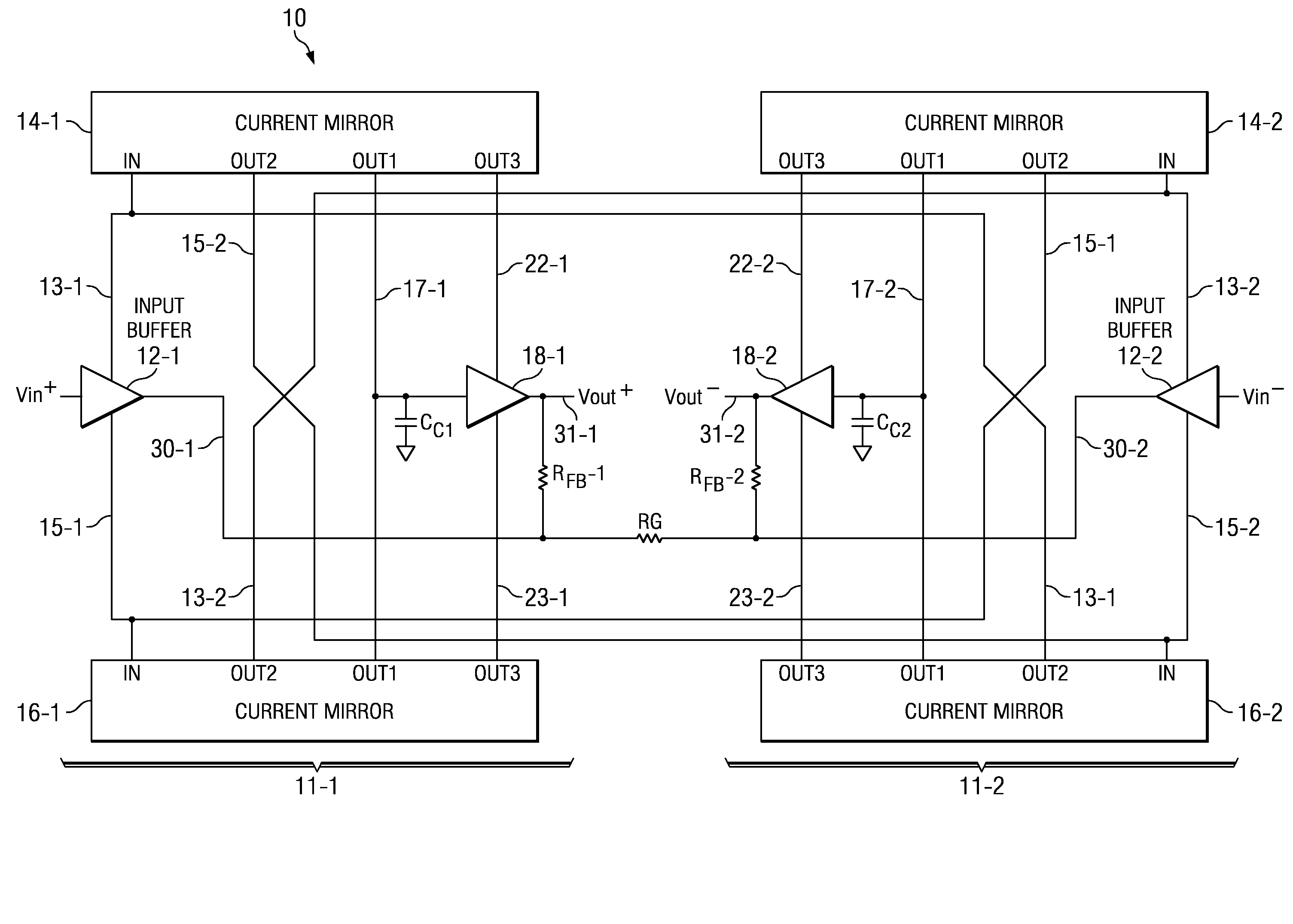
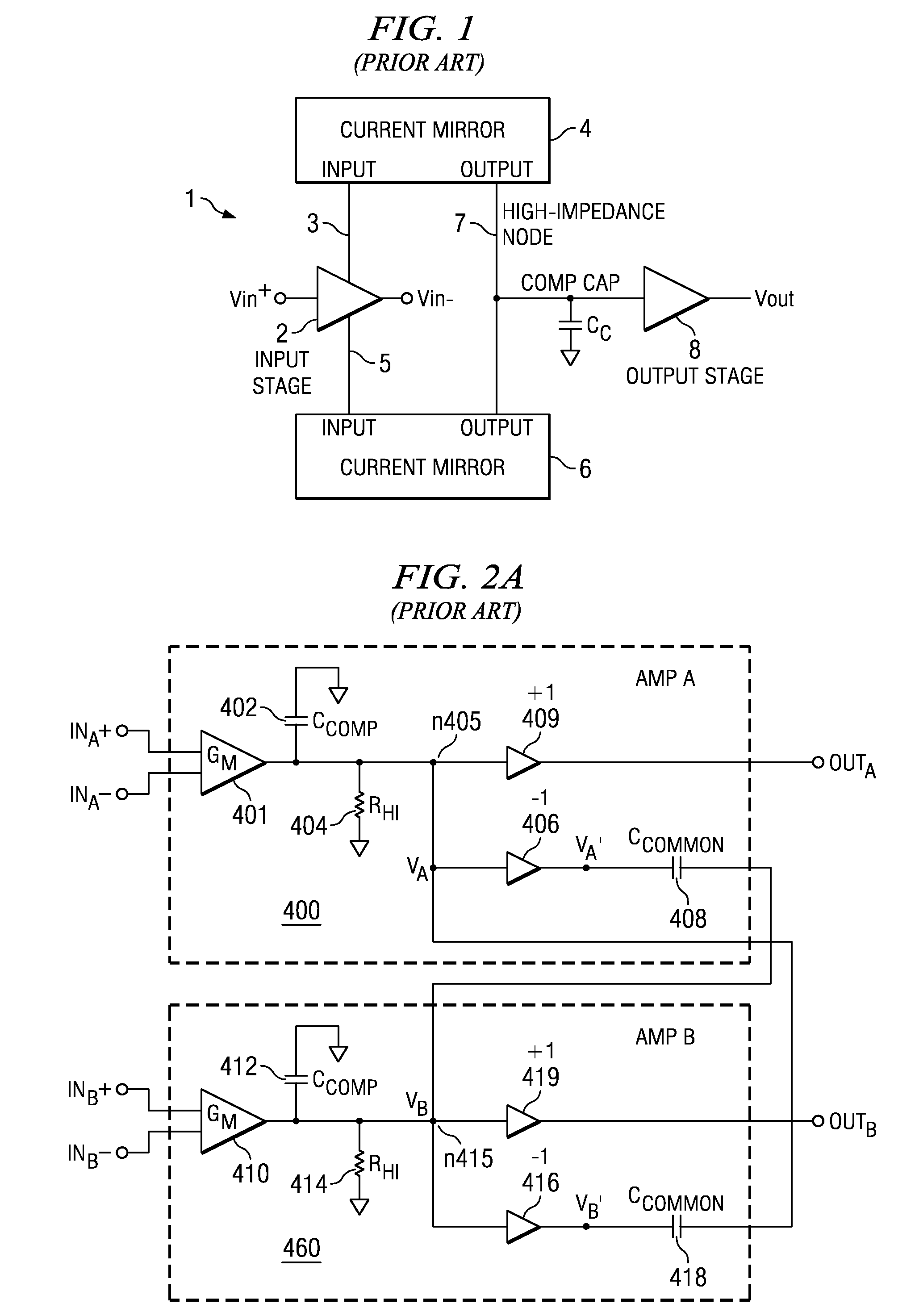
[0042]A proposed solution to the previously mentioned common mode instability problem in amplifier driver circuits is shown in FIG. 3. The typical current mirrors with one input and one output are replaced with current mirrors having one input and at least 2 outputs. The first outputs (OUT1) of each current feedback amplifier are connected together to form the high impedance node, which is the same as in a typical CFA. The second outputs (OUT2) of each current feedback amplifier, on the other hand, are connected to the opposite current mirror inputs of the complementary amplifier. These additional current mirror outputs function differently in relation to common mode and differential mode signals.

[0043]For differential mode signals, the voltage on the input of each current feedback amplifier is 180° out of phase with the voltage on the input of the other current feedback amplifier. Here the additional current mirror outputs in each current feedback amplifier will function symbiotica...


PUM


Abstract

An amplifier driver circuit (10) includes first (11-1) and second (11-2) feedback amplifiers including first (14-1) and second (14-2) upper current mirrors, respectively, and first (16-1) and second (16-2) lower current mirrors, respectively, first (12-1) and second (12-2) amplifier input stages receiving a common mode input signal, and first (18-1) and second (18-2) amplifier output stages coupled to outputs of the first and second amplifier input stages, respectively. Each current mirror has an input (IN) and first (OUT1) and second (OUT2) outputs. Upper bias terminals of the first (12-1) and second (12-2) amplifier input stages are coupled to the inputs (IN) of the first (14-1) and second (14-2) upper current mirrors, respectively, and are cross-coupled to the second outputs (OUT2) of the second (16-2) and first (16-1) lower current mirrors, respectively. Lower bias terminals of the first (12-1) and second (12-2) amplifier input stages are coupled to the inputs (IN) of the first (16-1) and second (16-2) lower current mirrors, respectively, and are cross-coupled to the second outputs (OUT2) of the second (14-2) and first (14-1) upper current mirrors, respectively, to oppose signals at the inputs (IN) of the current mirrors in response to the common mode input signal.

Description

CROSS REFERENCE TO RELATED APPLICATION[0001]This application claims the benefit of a first prior filed U.S. provisional application Serial No. 60 / 968,497 filed Aug. 28, 2007, entitled “Common Mode Bandwidth Reduction in Differential Applications”, by Paul G. Damitio and Ahmad Dashtestani, and incorporated herein by reference.BACKGROUND OF THE INVENTION[0002]The present invention relates generally to amplifier driver circuits, particularly to amplifier driver circuits composed of current feedback amplifiers, and more particularly to such amplifier driver circuits which avoid instability in response to both differential input signals and common-mode input signals. The invention also relates to amplifier driver circuits composed of voltage feedback amplifiers, and more particularly to such amplifier driver circuits which avoid instability in response to both differential input signals and common-mode input signals.[0003]Current feedback amplifiers (CFA) are generally considered to be t...

Claims


Application Information

Patent Timeline
Patent Type & Authority Patents(United States)
IPC IPC(8): H03F3/45
CPCH03F3/45085H03F3/45475H03F3/45479H03F3/45968H03F2203/45048H03F2203/45726H03F2203/45392H03F2203/45394H03F2203/45588H03F2203/45681H03F2203/45356
Inventor DAMITIO, PAUL G.DASHTESTANI, AHMAD
Owner TEXAS INSTR INC
Why Eureka
Try Eureka