

Semiconductor device with signal wirings that pass through under the output electrode pads and dummy wirings near the peripheral portion
a technology of semiconductor chips and signal wirings, applied in the direction of valves, oxygen/ozone/oxide/hydroxide, mechanical devices, etc., can solve the problem of difficult comparison of electrode pads' size, and achieve the effect of reducing the area of the semiconductor chip and enlarge the wiring area
- Summary
- Abstract
- Description
- Claims
- Application Information
AI Technical Summary
Benefits of technology
Problems solved by technology
Method used
Image

Examples
first embodiment
[0061]With reference to FIGS. 1 to 11, a description will be given below about a semiconductor device according to a first embodiment of the present invention applied to an LCD driver for which the reduction of the area of a semiconductor chip and a multi-output structure are required.
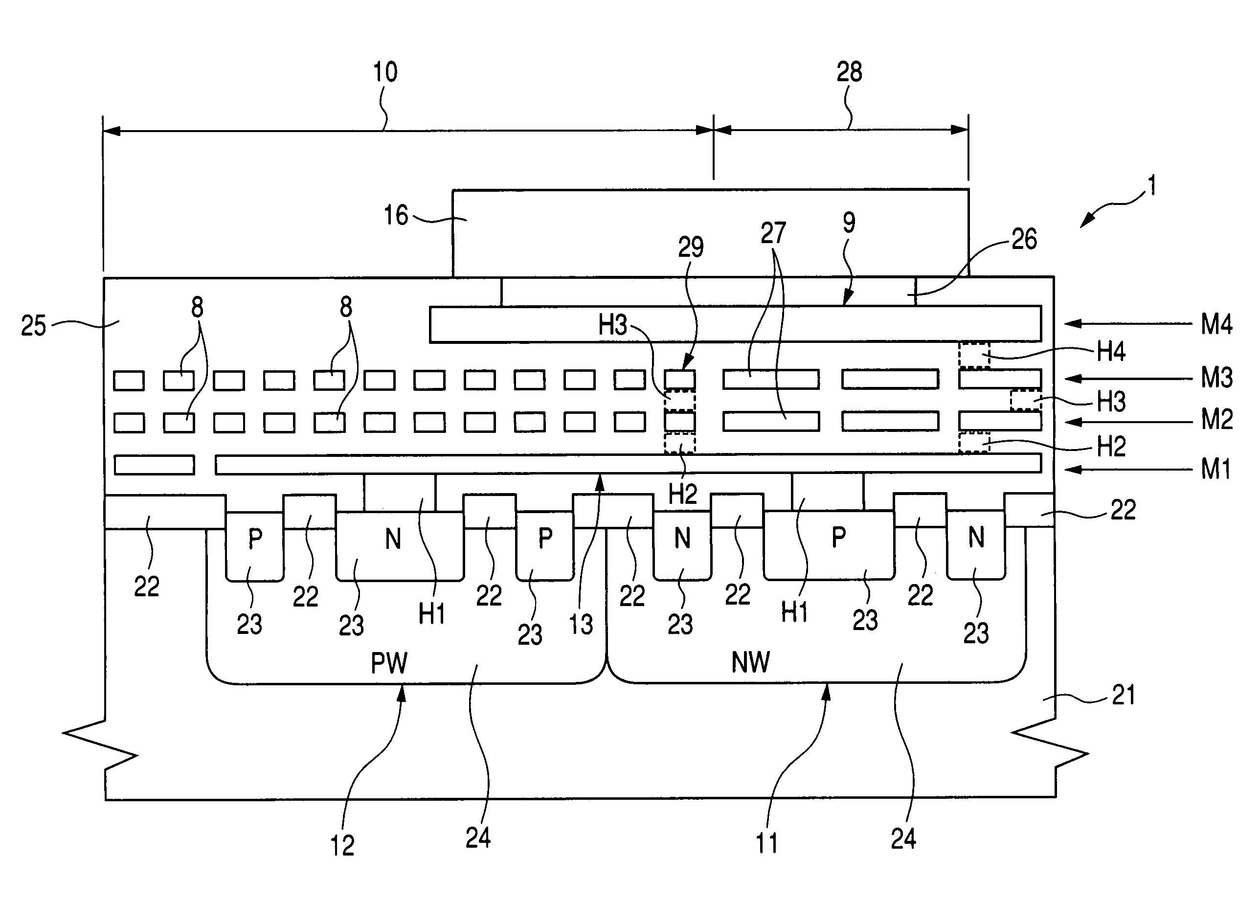
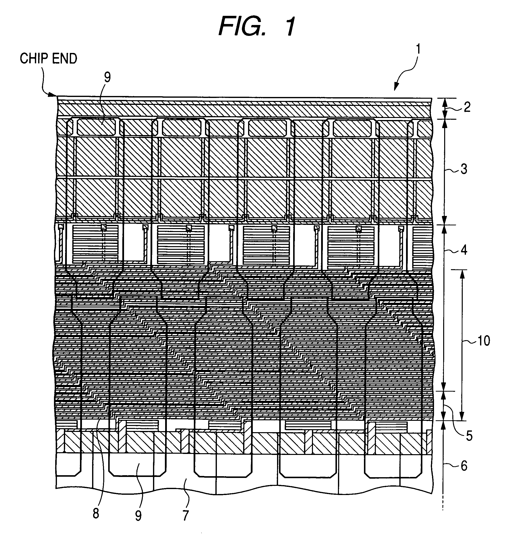
[0062]FIG. 1 is a plan view showing schematically a principal portion of the semiconductor device indicated at 1. Electrode pads 9 are also shown in the same figure in a see-through state.
[0063]On a main surface of a semiconductor chip of the semiconductor device 1, a scribe region 2, element region 3, element region 4, element isolation region 5 and element region 6 are arranged in this order from a chip end side toward a chip center side (in the vertical direction in FIG. 1).
[0064]The element region 6 is a region in which is formed an internal circuit 7 including, for example, MIS transistor and diodes. The element isolation region 5 is a region in which is formed, for example, LOCOS (local oxidation...
second embodiment
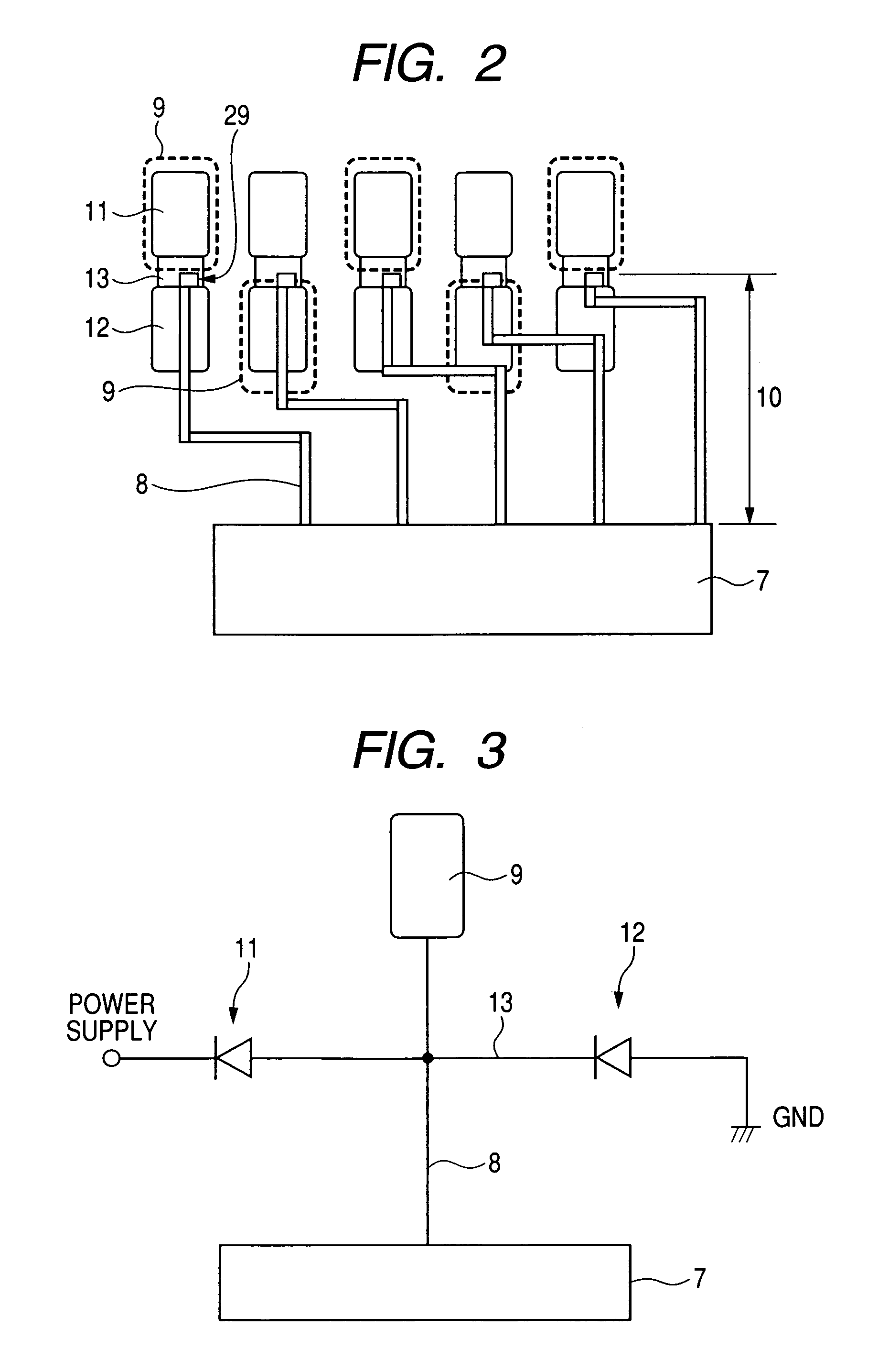
[0105]In the previous first embodiment, as shown in FIG. 2, the outlet ports 29 for the signal lines 8 are provided between the protective elements 11 and 12 in the semiconductor device having electrode pads 9 arranged in zigzags in two rows along a chip end side. In this second embodiment, a description will be given about a semiconductor device wherein outlet ports for the signal lines 8 are formed on a chip end side.
[0106]FIG. 12 is a plan view showing schematically a connection of principal portions in the semiconductor device according to this second embodiment, in which electrode pads 9 are shown in a see-through state.
[0107]As shown in FIG. 12, outlet ports 29 for signal lines 8 which provide electric connections from protective elements 11 and 12 to an internal circuit 7 are formed on a chip end side (the upper side in the vertical direction in FIG. 12) of the protective elements 11, whereby the signal lines 8 can be disposed over the protective elements 12 and further over ...
third embodiment
[0109]In the previous first embodiment, as shown in FIG. 2, the outlet ports 29 for the signal lines 8 are provided between the protective elements 11 and 12 in the semiconductor device having electrode pads 9 which are arranged in zigzags in two rows along a chip end side. In this third embodiment, a description will be given below about a semiconductor device having electrode pads 9 which are arranged straight in one row along a chip end side.
[0110]FIG. 13 is a plan view showing schematically a connection of principal portions in the semiconductor device according to this third embodiment, in which electrode pads 9 are shown in a see-through state.
[0111]As shown in FIG. 13, even in case of a straight layout of electrode pads 9, signal lines 8 which provide electric connections from the protective elements 11 and 12 to an internal circuit 7 can be drawn out from outlet ports 29 formed on wiring lines 13 located between the protective elements 11 and 12 and can be disposed over the ...
PUM
 Abstract
Description
Claims
Application Information