
Error detection/correction method

a technology of error detection and correction method, applied in the field of wafer-scale integrated circuit system, can solve the problems of failure of wafer-scale system, large part or the whole system is not functional, and its total area, and achieve high cache hit rate, high defect tolerance, and facilitate dynamic address mapping

Inactive Publication Date: 2009-12-15
MOSYS INC
View PDF194 Cites 11 Cited by
  • Summary
  • Abstract
  • Description
  • Claims
  • Application Information

AI Technical Summary

Benefits of technology

[0019]Accordingly, one object of this invention is to provide a defect or fault tolerant bus for connecting multiple functional modules to one or more bus masters, so that performance of the bus is not substantially affected by defects and faults in the bus nor in the modules.
[0022]Another object of this invention is to provide a method for changing the communication address of a module when the system is in operation. The technique facilitates dynamic address mapping and provides run-time fault tolerance to the system.
[0023]Another object of this invention is to provide programmability in the bus transceivers so that the bus network can be dynamically reconfigured.
[0025]In accordance with the present invention a high speed, fault-tolerant bus system is provided for communication between functional module and one or more bus controllers. Structured into a 3-level hierarchy, the bus allows high frequency operation (>500 MHz) while maintaining low communication latency (<30 ns), and high reconfiguration flexibility. Easy incorporation of redundant functional module and bus masters in the bus allows highly fault-tolerant systems to be built making the bus highly suitable for wafer-scale integrated systems. The bus employs a special source-synchronous block or packet transfer scheme for data communication and asynchronous handshakes for bus control and dynamic configuration. This source synchronous scheme allows modules to communicate at different frequencies and increases the overall yield of the system as it can accommodate both slow and fast memory devices without sacrificing the performance of the fast devices. It also frees the system of the burden of implementing a global clock synchronization which in general consumes a relatively large amount of power and is difficult to achieve high synchronization accuracy in a wafer-scale or large chip environment.
[0028]By grouping the DRAM arrays into logically independent modules of relatively small memory capacity (588 Kbit), a large number of cache lines (128) is obtained at small main memory capacity (4 Mbyte). The large number of cache lines is necessary for maintaining a high cache hit rate (>90%). The small module size also makes high-speed access (<30 ns) possible.
[0029]High defect tolerance in the hierarchical bus is obtained using the following techniques: 1) Use of relatively small block size (512 K bit or 588 K bit with parity) for the memory modules; 2) Use of programmable identification register to facilitate dynamic address mapping and relatively easy incorporation of global redundancy; 3) Use of a grid structure for the bus to provide global redundancy for the interconnect network; 4) Use of a relatively narrow bus consisting of 13 signal lines to keep the total area occupied by the bus small; 5) Use of segmented bus lines connected by programmable switches and programmable bus transceivers to facilitate easy isolation of bus defects; 6) Use of special circuit for bus transceivers and asynchronous handshakes to facilitate dynamic bus configuration; 7) Use of programmable control register to facilitate run-time bus reconfiguration; 8) Use of spare bus lines to provide local redundancy for the bus; and 9) Use of spare rows and columns in the memory module to provide local redundancy.

Problems solved by technology

The major barrier to a successful wafer-scale system has been defects inherent in the fabrication process which may render a substantial part of or the whole system nonfunctional.
Since the network may extend over the entire wafer, its total area is significant and it is highly susceptible to defects.
Traditionally, high communication performance and defect tolerance are conflicting requirements on the network.
High communication performance, such as short latency and high bandwidth, requires large numbers of parallel lines in the network which occupy a large area, making it more susceptible to defects.
However, they inherit the disadvantage of a serial bus and suffer from long access latency because the communication signals have to be relayed from one block to another down the serial bus.
However, a parallel bus system without reconfiguration capability offers the lowest defect tolerance since any defect on the bus can render a substantial part of the system without communication link.
Known systems implement parallel bus with limited success.
Without redundancy and reconfiguration capability in the bus, harvest rate is relatively low, because defects in the main bus can still cause failure in a substantial part of the system.
This complicates the overall defect management of the system as a whole and increases the total interconnect overhead.
The separation of address and data buses increases the bus overhead and complicates the defect management.

Method used


Image

  • Error detection/correction method
  • Error detection/correction method
  • Error detection/correction method

Examples


Embodiment Construction

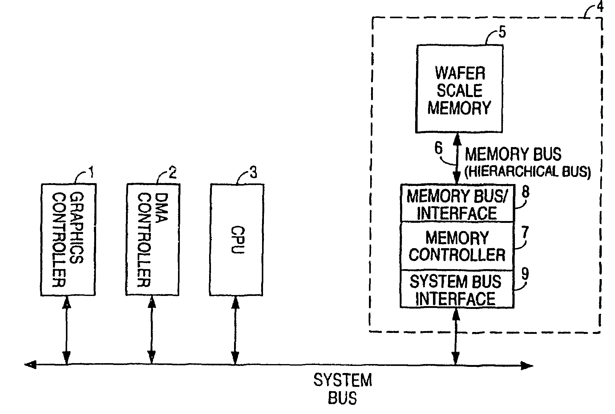
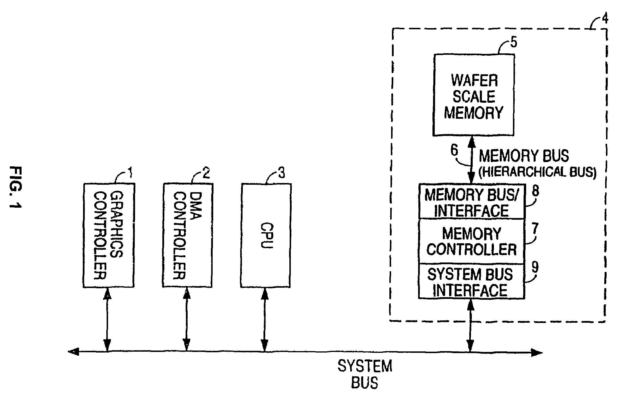
[0058]As illustrated in FIG. 1, a memory sub-system according to the present invention is used in a digital system, which consists of a wafer scale memory 5, hierarchical memory bus 6 and a memory controller 7. The memory controller 7 controls memory access and comprises a memory bus interface 8 for communicating to the hierarchical bus 6, and a system bus interface 9 for communicating to the system bus 10. The system bus 10 connects the memory subsystem to the memory request devices which are CPU 3, DMA controller 2 and graphics controller 1.

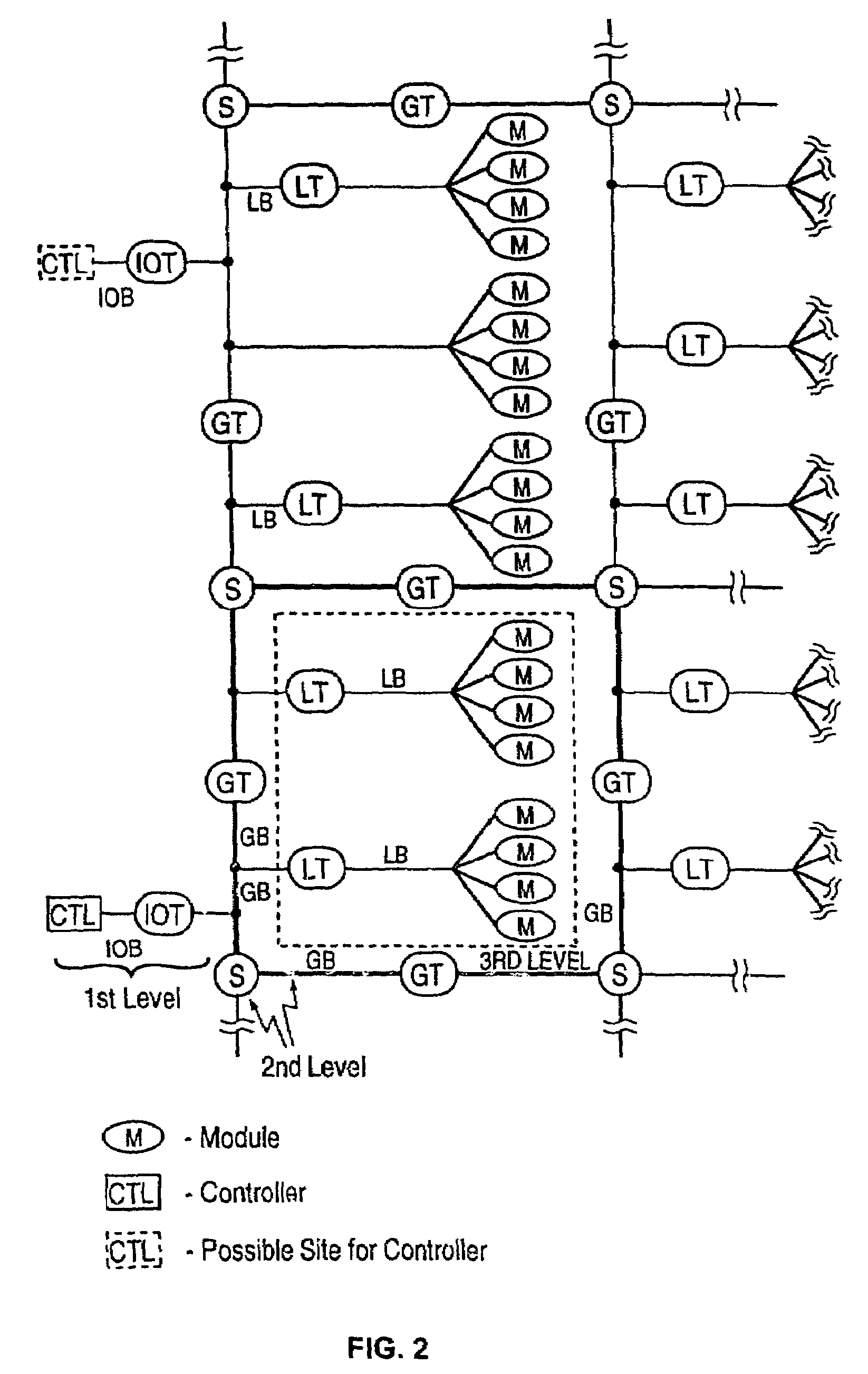
[0059]The bus has a hierarchical structure which can be distinguished into 3 levels. As illustrated in FIG. 2, the first level or the root level has a few branches (IOB) for connecting the memory controller to the second level. In most cases, only one branch is used for the connection, unless multiple controllers are used, the other branches are used for spares. The root branches (IOB) are connected to the second level through the input-output ...


PUM


Abstract

A method for error detection and correction (EDC) includes: generating a complete EDC code in response to a data packet; distributing the complete EDC code among the data packet to create a plurality of bytes, each including a data portion from the data packet and an EDC code portion from the complete EDC code; storing the bytes in a memory module; retrieving the bytes from the memory module; forwarding the data portions of the bytes retrieved from the memory module to a requesting device; providing the data portions of the bytes retrieved from the memory module to an EDC functional block; providing the EDC code portions of the bytes retrieved from the memory module to the EDC functional block; and performing error checking and correction in the EDC functional block upon receiving the complete EDC code from the provided EDC code portions.

Description

CROSS-REFERENCE TO RELATED APPLICATIONS[0001]This application is a divisional of U.S. patent application Ser. No. 10 / 273,442 entitled “Latched Sense Amplifiers As High Speed Memory In A Memory System” filed Oct. 15, 2002 now U.S. Pat. No. 6,717,864 by Leung et al.;[0002]which is a continuation of U.S. patent application Ser. No. 09 / 903,094 (now U.S. Pat. No. 6,483,755) entitled “Memory Modules With High Speed Latched Sensed Amplifiers” filed Jul. 10, 2001 by Leung et al.;[0003]which is a continuation of U.S. patent application Ser. No. 08 / 820,297 (now U.S. Pat. No. 6,425,046) entitled “Method For Using A Latched Sense Amplifier In A Memory Module As a High-Speed Cache Memory” filed 18 Mar. 1997 by Leung et al.;[0004]which is a divisional of U.S. patent application Ser. No. 08 / 484,063 (now U.S. Pat. No. 5,666,480 entitled “Fault-Tolerant Hierarchical Bus System And Method of Operating Same,” filed Jun. 6, 1995 by Leung et al.;[0005]which is a divisional of U.S. patent application Ser...

Claims


Application Information

Patent Timeline
Patent Type & Authority Patents(United States)
IPC IPC(8): H03M13/00G11C29/00G06F12/16G06F11/00G06F11/10G06F11/20G06F12/06G06F13/00G06F13/40G11C29/04G11C29/48H01L21/66H01L27/02H04L5/14H04L25/02
CPCG06F11/1032G06F11/2007G06F12/0661G06F13/4077G11C29/006G11C29/08G11C29/48G11C29/76G11C29/808G11C29/832G11C29/88H01L22/22H04L5/1461H04L25/026H04L25/0272G06F11/10G06F11/006Y10S257/907G11C5/04G11C29/81G11C2029/0401G11C2029/0411G11C2029/4402H01L27/0203H04L25/028H04L25/029H04L25/0292
Inventor LEUNG, WINGYUHSU, FU-CHIEH
Owner MOSYS INC
Learn More