Error Detection/Correction Method

a technology of error detection and correction method, applied in the field of wafer-scale integrated circuit system, can solve the problems of failure of wafer-scale system, large part or the whole system is not functional, and its total area, and achieve high cache hit rate, high defect tolerance, and facilitate dynamic address mapping

a technology of error detection and correction method, applied in the field of wafer-scale integrated circuit system, can solve the problems of failure of wafer-scale system, large part or the whole system is not functional, and its total area, and achieve high cache hit rate, high defect tolerance, and facilitate dynamic address mapping

US20080209303A1Inactive Publication Date: 2008-08-28MOSYS INC

Image

  • Error Detection/Correction Method
  • Error Detection/Correction Method
  • Error Detection/Correction Method

Examples


Embodiment Construction

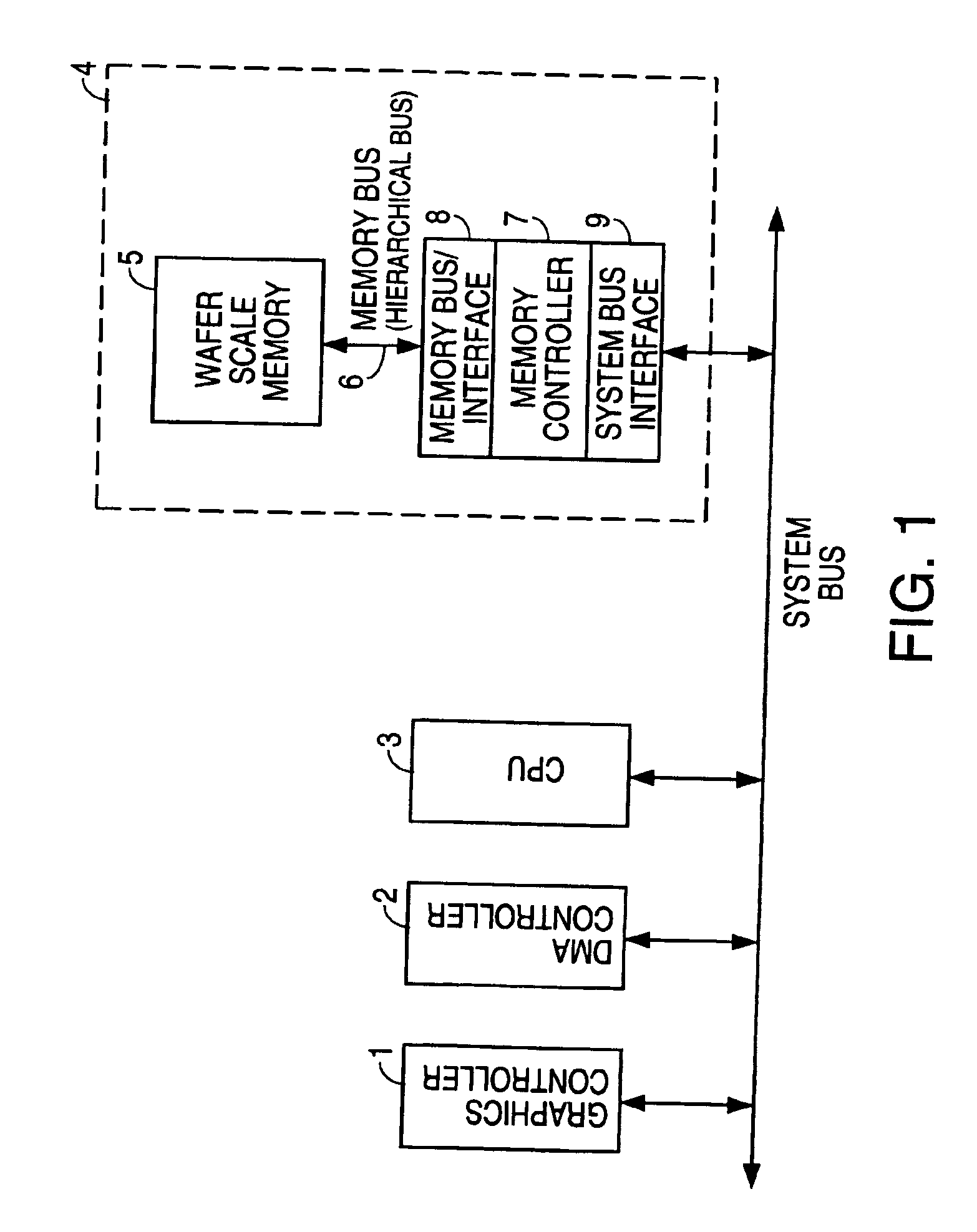
[0059]As illustrated in FIG. 1, a memory sub-system according to the present invention is used in a digital system, which consists of a wafer scale memory 5, hierarchical memory bus 6 and a memory controller 7. The memory controller 7 controls memory access and comprises a memory bus interface 8 for communicating to the hierarchical bus 6, and a system bus interface 9 for communicating to the system bus 10. The system bus 10 connects the memory subsystem to the memory request devices which are CPU 3, DMA controller 2 and graphics controller 1.

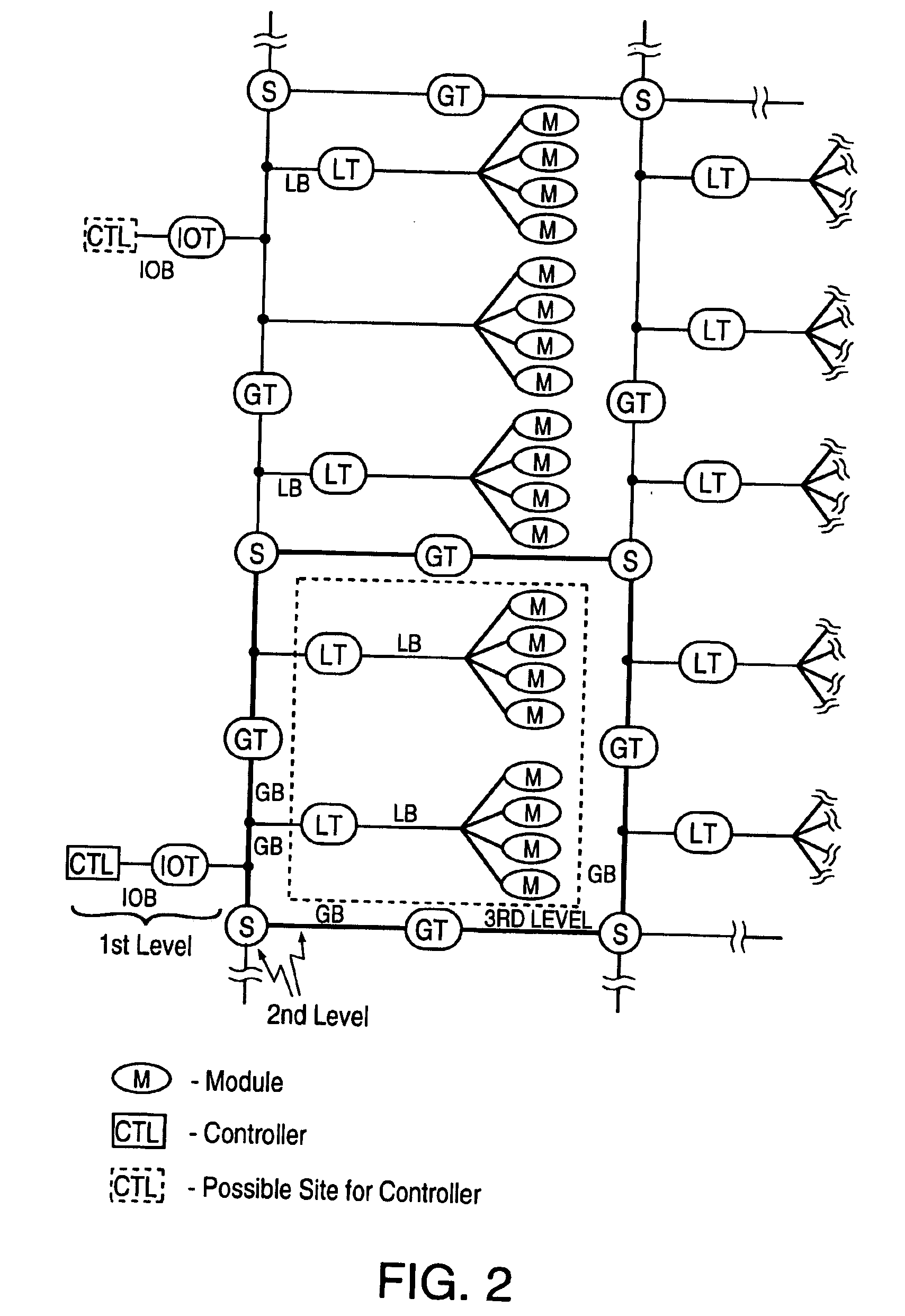
[0060]The bus has a hierarchical structure which can be distinguished into 3 levels. As illustrated in FIG. 2, the first level or the root level has a few branches (IOB) for connecting the memory controller to the second level. In most cases, only one branch is used for the connection, unless multiple controllers are used, the other branches are used for spares. The root branches (IOB) are connected to the second level through the input-output ...


PUM


Abstract

A method for error detection and correction (EDC) includes: generating a complete EDC code in response to a data packet; distributing the complete EDC code among the data packet to create a plurality of bytes, each including a data portion from the data packet and an EDC code portion from the complete EDC code; storing the bytes in a memory module; retrieving the bytes from the memory module; forwarding the data portions of the bytes retrieved from the memory module to a requesting device; providing the data portions of the bytes retrieved from the memory module to an EDC functional block; providing the EDC code portions of the bytes retrieved from the memory module to the EDC functional block; and performing error checking and correction in the EDC functional block upon receiving the complete EDC code from the provided EDC code portions.

Description

CROSS-REFERENCE TO RELATED APPLICATIONS[0001]This application is a divisional of U.S. patent application Ser. No. 10 / 800,382 entitled “Error Detection / Correction Method” (as amended) filed Mar. 11, 2004 by Leung et al.;[0002]This application is a divisional of U.S. patent application Ser. No. 10 / 273,442 (now U.S. Pat. No. 6,717,864) entitled “Latched Sense Amplifiers As High Speed Memory In A Memory System” filed Oct. 15, 2002 by Leung et al.;[0003]which is a continuation of U.S. patent application Ser. No. 09 / 903,094 (now U.S. Pat. No. 6,483,755) entitled “Memory Modules With High Speed Latched Sensed Amplifiers” filed Jul. 10, 2001 by Leung et al.;[0004]which is a continuation of U.S. patent application Ser. No. 08 / 820,297 (now U.S. Pat. No. 6,425,046) entitled “Method For Using A Latched Sense Amplifier In A Memory Module As a High-Speed Cache Memory” filed 18 Mar. 1997 by Leung et al.;[0005]which is a divisional of U.S. patent application Ser. No. 08 / 484,063 (now U.S. Pat. No. 5...

Claims


Application Information

Patent Timeline
28 Aug 2008
Publication
US20080209303A1
IPC
H03M13/05; G06F11/10; G06F12/16; G06F11/00; G06F11/20; G06F12/06; G06F13/00; G06F13/40; G11C29/00; G11C29/04; G11C29/48; H01L21/66; H01L27/02; H04L5/14; H04L25/02
CPC
G06F11/006; Y10S257/907; G06F11/1032; G06F11/2007; G06F12/0661; G06F13/4077; G11C5/04; G11C29/006
Inventors
LEUNG, WINGYU; HSU, FU-CHIEH